Pin correcting device for integrated circuit

A technology of integrated circuits and calibration devices, which is applied in the direction of assembling printed circuits, electrical components, electrical components, etc., which can solve the problems of complex structure and high manufacturing/purchase costs, and achieve simple calibration process, reduce purchase costs, and reduce production / Repair cost effect

Inactive Publication Date: 2010-01-20
上海允科自动化有限公司
View PDF2 Cites 13 Cited by
  • Summary
  • Abstract
  • Description
  • Claims
  • Application Information

AI Technical Summary

Problems solved by technology

The work efficiency of the whole device is high, and it is suitable for the operation line of mass production, but it has the disadvantages of complex structure and high manufacturing / purchase cost. Similarly, the integrated circuit after its whole pin can only be used for insertion PCB board production process and cannot be used for patch production process

Method used


Image

  • Pin correcting device for integrated circuit
  • Pin correcting device for integrated circuit
  • Pin correcting device for integrated circuit

Examples


Embodiment Construction

[0021] The integrated circuit pin correction device of the present invention will be further described below in conjunction with the accompanying drawings.

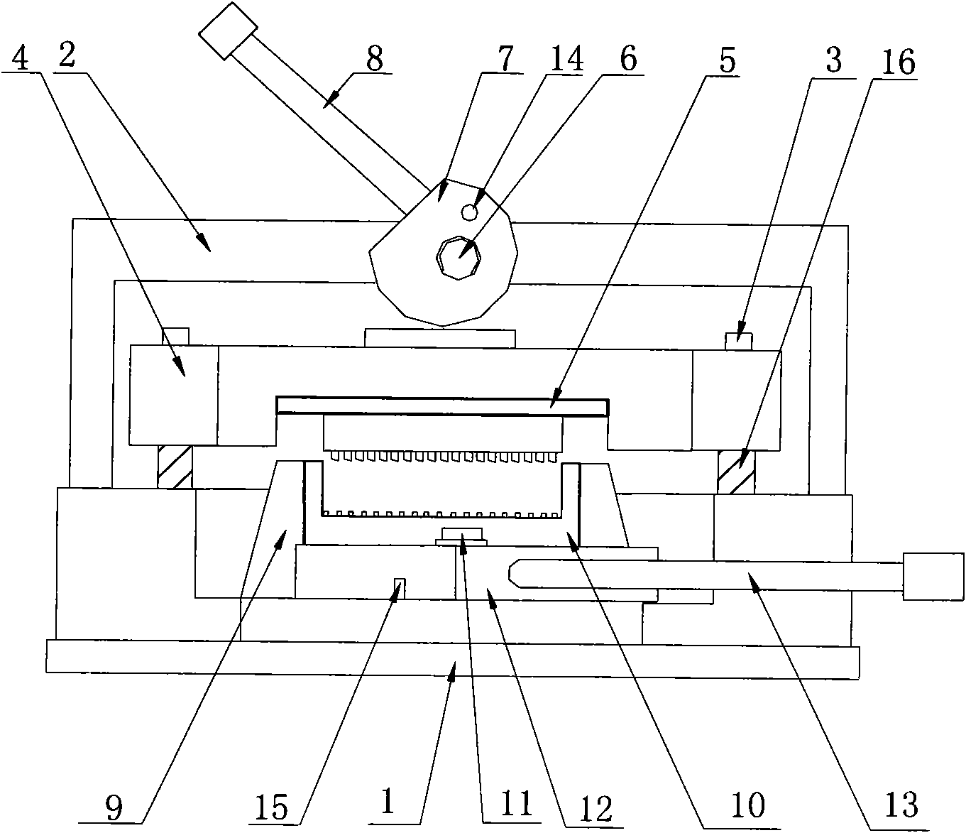
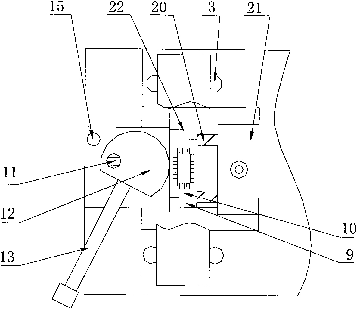
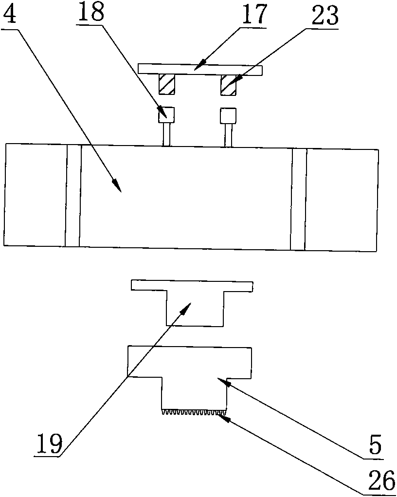
[0022] figure 1 Among them, a base 1 is included, and a gantry 2 is arranged on the base; a guide post 3 and an upper module block 4, 5 that can move longitudinally along the guide post are set on the base below the gantry; The first eccentric wheel assembly 6, 7, 8 that can drive the upper module block to move longitudinally is set on the frame 2; the second eccentric wheel assembly 11, 12, which can drive the lower module to move laterally is set on the base under the portal frame. 13.

[0023] Wherein, on the guide column 3 between the base and the upper module block, a first return spring 16 is arranged.

[0024] The first eccentric wheel assembly includes a first fixed shaft 6 arranged on the portal frame 2, a first eccentric wheel 7 located on the first fixed shaft, and a first operating handle 8 arranged on the s...


PUM


Abstract

The invention discloses a pin correcting device for an integrated circuit, and belongs to the field of treating semiconductor components and equipment. The pin correcting device comprises a pedestal; a door-shaped frame is arranged on the pedestal; a guide post and an upper module block which can move longitudinally along the guide post are arranged on the pedestal under the door-shaped frame; a first eccentric wheel component which can drive the upper module block to move longitudinally is arranged on the door-shaped frame; a slide way, a lower module block which can move transversely along the slide way and a second eccentric wheel component which can drive the lower module block to move transversely are arranged on the pedestal under the door-shaped frame; and one end of the slide way is provided with a limit block. The upper module block and the lower module block are set as separable structures, so that a correcting process for a pin is simple and accurate; the requirements of users are fully considered, and the acquisition expenses and production / maintenance costs for enterprises can be reduced; and the corrected integrated circuit can completely pass the detection of automatic detection equipment, and can be applied to a patch production process. The pin correcting device for the integrated circuit can be widely applied in the pretreatment fields of pin reforming of various integrated circuits and the patch production process.

Description

technical field [0001] The invention belongs to the field of methods or equipment suitable for manufacturing or processing semiconductor or solid devices or parts thereof, and in particular relates to a device for correcting packaged integrated circuit pins with defective pins. Background technique [0002] After the integrated circuit chip (abbreviated as integrated circuit, the same below) is packaged, the integrated circuit will be soldered or pasted on the circuit board (commonly known as PCB board) as a chip component. Among them, the pins of the integrated circuit (also called pins, the same below) serve as a bridge connecting the internal circuit of the integrated circuit with the circuit board circuit, and have extremely strict requirements on its size. There are many types of integrated circuits, and some have fewer pins, which are relatively easy to handle; however, some integrated circuits have many and dense pins, and the distance between the pins of the packaged...

Claims


Application Information

Patent Timeline
Patent Type & Authority Applications(China)
IPC IPC(8): H05K13/00H05K3/30
Inventor 柯恩清王东
Owner 上海允科自动化有限公司
Why Eureka
Try Eureka