Storage and transfer of organic nanofibers

An organic nanofiber, nanofiber technology, used in transportation and packaging, electrical components, circuits, etc., to solve storage-related problems

Inactive Publication Date: 2010-01-20
NANOFIBER
View PDF1 Cites 2 Cited by
  • Summary
  • Abstract
  • Description
  • Claims
  • Application Information

AI Technical Summary

Problems solved by technology

In this case, between the production of active components and their introduction into electronic devices, problems related to the storage of nano- or sub-micron-sized components or devices produced on the first substrate may arise

Method used


Image

  • Storage and transfer of organic nanofibers
  • Storage and transfer of organic nanofibers
  • Storage and transfer of organic nanofibers

Examples


Embodiment Construction

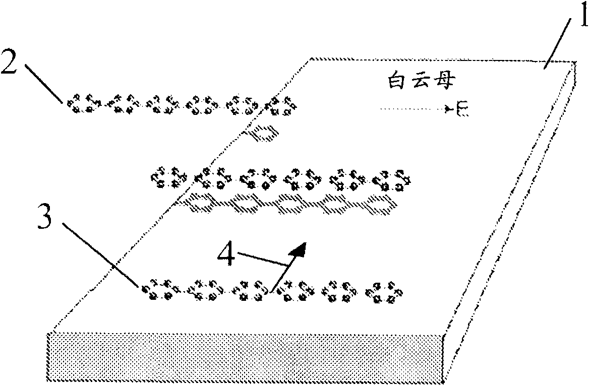
[0060] Embodiments of the invention relate to the transfer of nanofibers from a template substrate to a flexible storage medium. In a step prior to the transfer process, a template substrate loaded with nanofibers and a flexible storage medium are provided.

[0061] figure 1 and figure 2 A possible template substrate and an embodiment of nanofibers in the form of elongated arrays of nanofibers of organic molecules grown on a mica substrate are described.

[0062] figure 1 The growth of organic nanofibers2, 3 on a template substrate, or more specifically, the growth of phenylene nanofibers on a muscovite substrate, is briefly illustrated.

[0063] Mica can be prepared such that an electric field appears on the surface, for example by cleaving in air and immediately transferring to a vacuum device which can be degassed, for example at 410K for 0.5 hours or possibly longer; split directly.

[0064] The nanofibers presented in this section are made of p-phenylene oligomers (...


PUM

PropertyMeasurementUnit
widthaaaaaaaaaa

Abstract

The present invention relates to a method of transferring nanofibres from a template substrate to a flexible storage medium. The method comprising : a) providing the template substrate supporting nanofibres and the flexible storage medium; b) positioning the flexible storage medium so that a first storage area of the flexible storage medium is facing a first support area of the template substrate; and c) pressing the first storage area of the flexible storage medium in contact with the first support area of the template substrate and remove the first storage area of the flexible storage medium from contact with the first support area of the template substrate, thereby transferring the nanofibres from the template substrate to the flexible storage medium and thereby providing a loaded flexible storage medium. The present invention is advantageous for providing a method of storing and handling of nanofibres for commercial implementation into working devices, by providing a solution to problems concerning compact storage of nanofibres for further use.

Description

field of invention [0001] The present invention relates to the storage of nanofibers, and in particular to the transfer of nanofibers from a template substrate to a storage medium. Background of the invention [0002] The current rapid miniaturization of optoelectronics has led to increasing interest in the production, characterization and connection of optoelectronic components with sub-micrometer or nanometer length feature dimensions. Requirements for optically active elements in submicron or nanoscale optoelectronic devices include such things as easy optical tunability, strong luminous efficiency, flexibility of molecular-based elements, and that light should be generated and propagated in a predetermined manner. Organic optically active elements can meet the requirements. [0003] A common difficulty is that it is impossible, inconvenient or economically infeasible to form organic submicron or nanoscale optically active elements or devices directly on the desired subs...

Claims


Application Information

Patent Timeline
Patent Type & Authority Applications(China)
IPC IPC(8): H01L51/56
CPCH01L51/003H01L51/0013H01L51/0038Y10T428/24479H10K71/18H10K71/80H10K85/114
Inventor 霍斯特贡特·鲁巴恩卡斯珀·蒂尔辛-汉森
Owner NANOFIBER
Why Eureka
Try Eureka