Mini-size package lead frame structure and processing method thereof

A technology for encapsulating lead and frame structure, applied in electrical components, electrical solid devices, circuits, etc., can solve the problems of inability to realize exposed heat dissipation plate, difficult to achieve, and high cost, and achieve high reliability, low cost, and guaranteed reliability. Effect

Active Publication Date: 2010-01-27
LESHAN PHOENIX SEMICON
View PDF0 Cites 6 Cited by
  • Summary
  • Abstract
  • Description
  • Claims
  • Application Information

AI Technical Summary

Problems solved by technology

At present, the exposed heat dissipation pad package is mainly used on larger-sized IC packages, but the exposed heat dissipation pad design cannot be realized on the micro package due t

Method used


Image

  • Mini-size package lead frame structure and processing method thereof
  • Mini-size package lead frame structure and processing method thereof
  • Mini-size package lead frame structure and processing method thereof

Examples


Embodiment Construction

[0017] The present invention will be further described in detail below in conjunction with the accompanying drawings and specific embodiments.

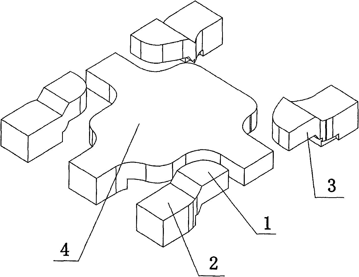
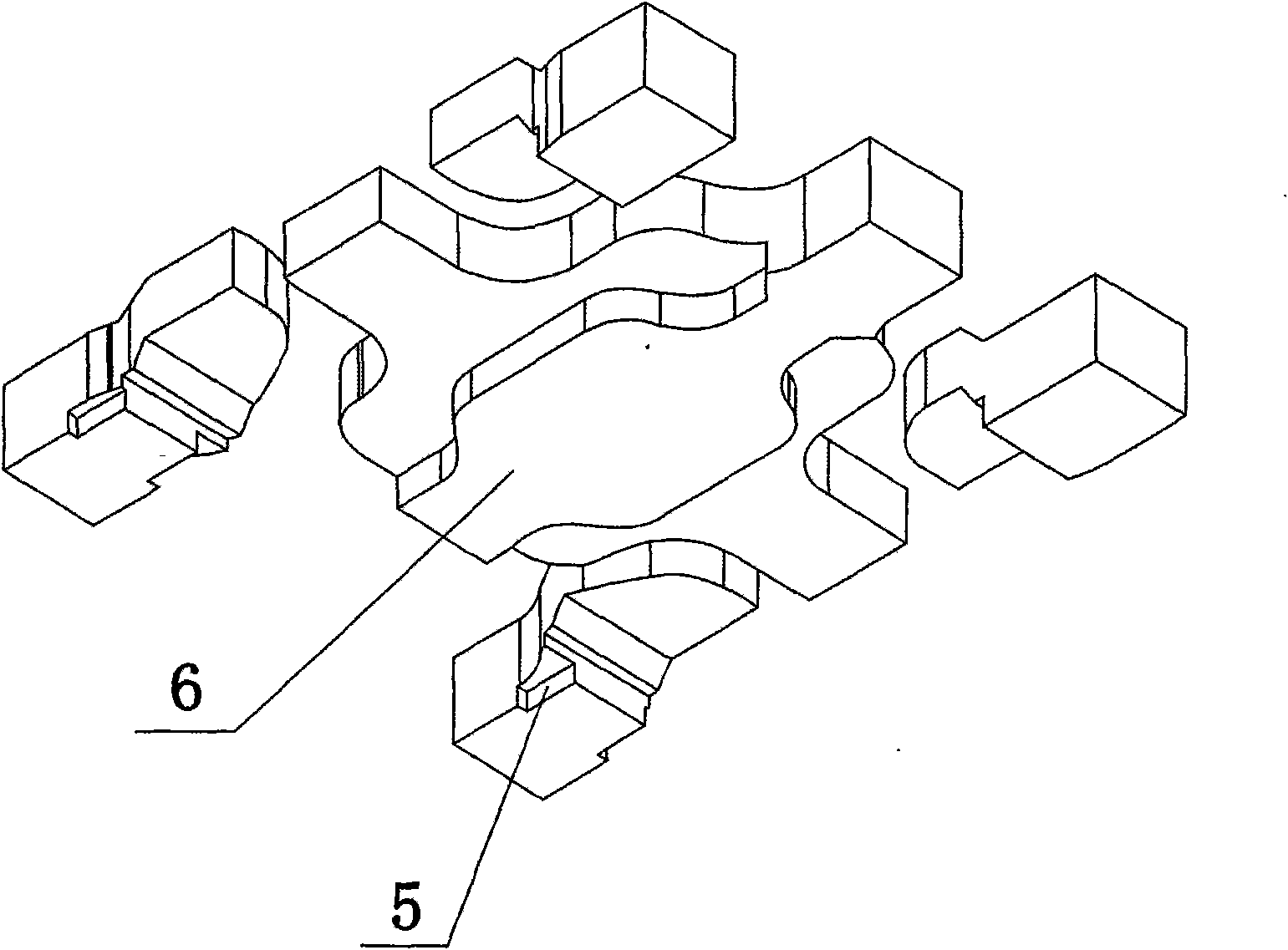
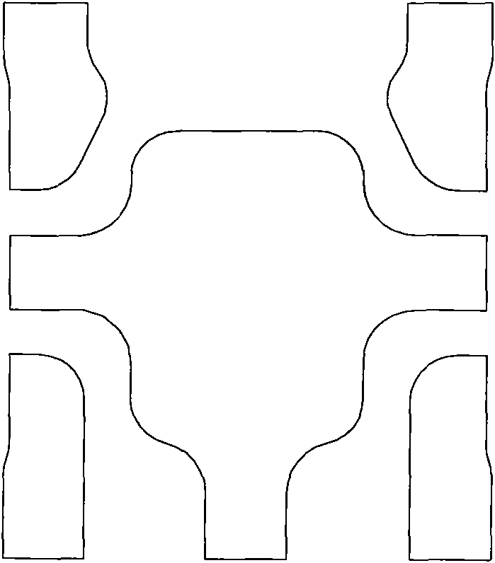
[0018] Such as figure 1 and figure 2 As shown, a micro-package lead frame structure includes a chip bonding area 4 and four lead inner frames surrounding the chip bonding area 4, and the lead inner frame is provided with an outer pin 2, an inner pin mold-locking structure 3 and The inner pin bonding area 1, the back side of the chip bonding area 4 is provided with an exposed cooling plate 6, and the inner frame of the lead is also provided with an outer pin mold lock structure 5, and the outer pin mold lock structure 5 is the outer pin 2 The slots on the corners on both sides of the pins. The exposed heat dissipation plate 6 is a raised area on the back of the chip bonding area 4 , and is integrally formed with the chip bonding area 4 . The thickness of the exposed cooling plate 6 is fifty microns. The inner pin bonding area 1 is...


PUM


Abstract

The invention discloses a mini-size package lead frame structure and a processing method thereof. The mini-size package lead frame structure comprises a chip welding area and a lead wire inner frame, the lead wire inner frame is provided with an outer pin, an inner pin mold locking structure and an inner pin welding wire area, the reverse of the chip welding area is provided with an exposed radiating disk, the lead wire inner frame is further provided with an outer pin mold locking structure, and the outer pin mold locking structure is a groove arranged at two lateral angles of the outer pin. The processing method of the mini-size package lead frame comprises the following steps: performing die-cutting and molding on a base material to form outer contours of an inner pin, the outer pin and the chip welding area; performing deep stamping to form the inner pin, the outer pin, the exposed radiating disk and the chip welding area, and initially forming the shape and the structure of the inner pin welding wire area; performing the deep stamping to form the outer pin mold locking structure; and bending and molding to form the inner pin welding wire area and the inner pin mold locking structure. The invention has low cost and high reliability, realizes the plastic package of a chip with higher power on the mini-size package and provides a development platform for the mini-size package of the exposed radiating disk.

Description

technical field [0001] The invention relates to the technical field of integrated circuit packaging, in particular to a micro-package lead frame structure and a process method thereof. Background technique [0002] Lead frame is one of the most important and basic packaging materials in the field of semiconductor plastic packaging. The main packaging materials in semiconductor plastic packaging are: lead frame, plastic packaging compound, chip and lead. The lead frame supports the entire package body in the whole package body, and its structural design is particularly important. First of all, the chip welding area of ​​the lead frame should support the chip, provide the welding area of ​​the chip, and also be the electrical conduction inside the package, the electrical conduction between the device and the circuit board, and the heat conduction between the device and the circuit board when it is working. At present, micro-packages developed to meet the requirements of smal...

Claims


Application Information

Patent Timeline
IPC IPC(8): H01L23/495H01L23/367H01L21/48
CPCH01L2924/0002
Inventor 曾德鑫王廉发潘强华
Owner LESHAN PHOENIX SEMICON
Why Eureka
Try Eureka