Optical waveguide and spot size converter using this

一种光波导、模转换的技术,应用在光波导的耦合、光导、光学等方向,能够解决难以将模直径调整光纤等问题

Inactive Publication Date: 2010-02-03
NEC CORP
View PDF13 Cites 50 Cited by
  • Summary
  • Abstract
  • Description
  • Claims
  • Application Information

AI Technical Summary

Problems solved by technology

[0005] However, the Δ of the optical waveguide gradually increases as the size of the optical waveguide device decreases, and according to the above method, the processing size of the optical waveguide needs to be very fine and very precise
Therefore, it becomes difficult to adjust the mode diameter to the diameter of the fiber

Method used


Image

  • Optical waveguide and spot size converter using this
  • Optical waveguide and spot size converter using this
  • Optical waveguide and spot size converter using this

Examples


example 1

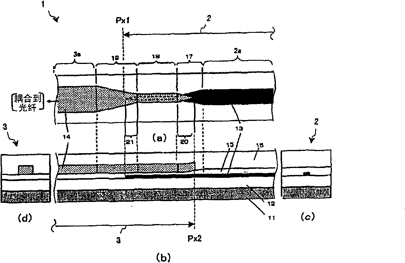
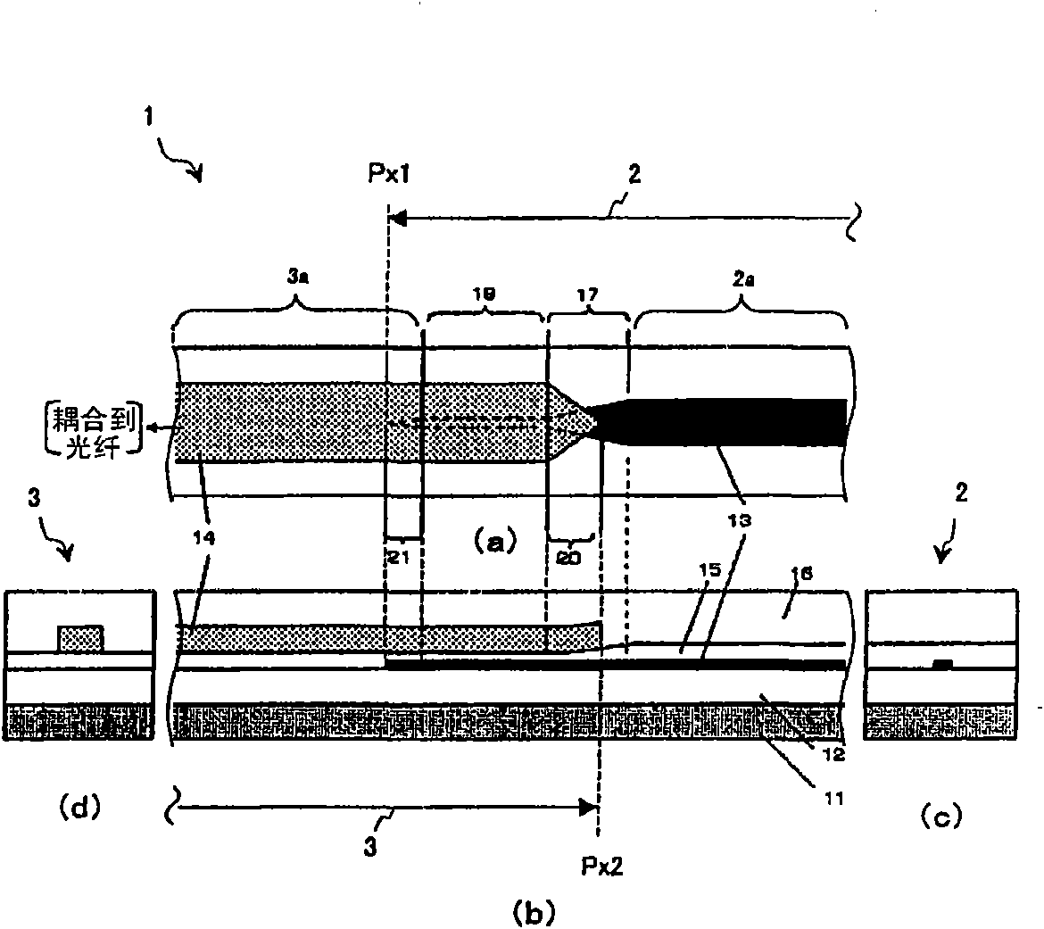
[0057] figure 1 is a schematic diagram schematically showing an example of the configuration of the spot size converter using the optical waveguide 1 according to the first example of the present invention. figure 1 A is a cross-sectional view of the main part of the upper surface. figure 1 B is a cross-sectional view of the main part of the plane. figure 1 C is a cross-sectional view of the main part of the right side. figure 1 D is a sectional view of the main part of the left side. Incidentally, figure 1 A and figure 1 B shows the cross-sectional surface of the main part of the optical waveguide 1 . As shown by the wavy lines in the figure, both ends of the optical waveguide 1 are not limited to the end faces of the actual waveguide chip. Furthermore, in the case of the example shown by this figure, the optical waveguide 1 is coupled with an optical fiber. Alternatively, the optical waveguide 1 can be applied to other cases such as when the optical waveguide 1 is cou...

example 2

[0074] Next, a second example of the present invention will be described in detail with reference to the drawings.

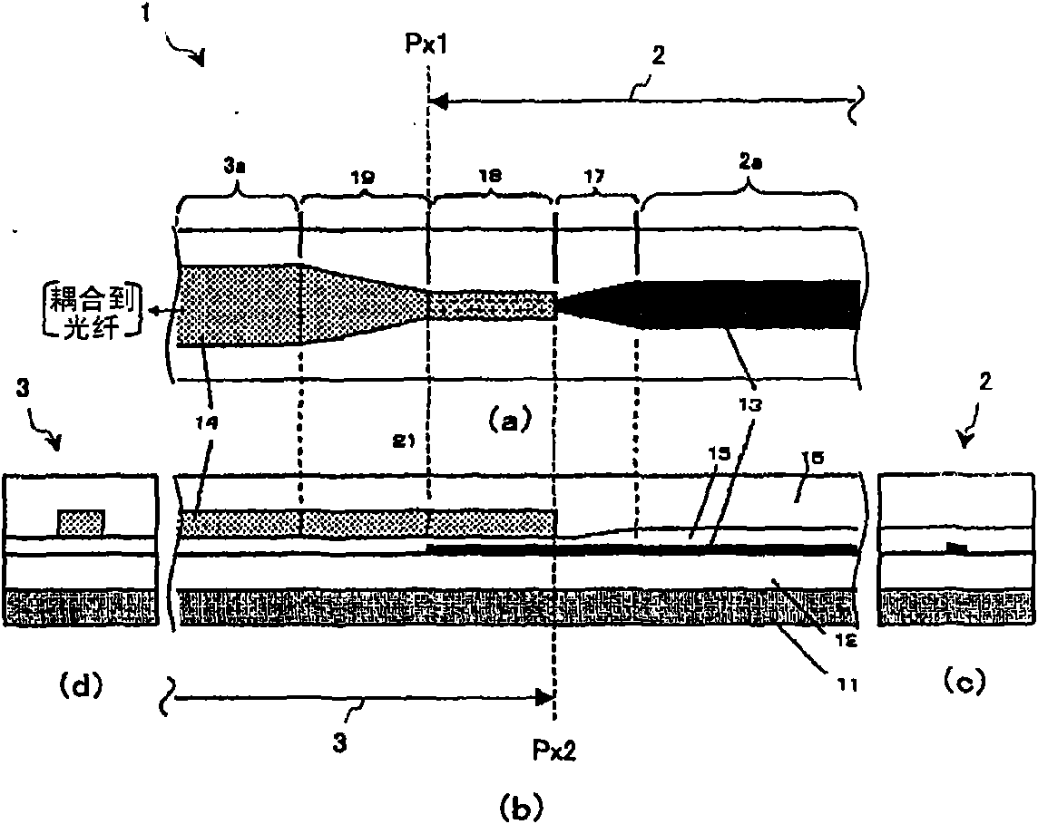
[0075] figure 2 is a schematic diagram schematically showing an example of the structure of the optical waveguide 1 according to the present example. figure 2 A is a cross-sectional view of the main part of the upper surface. figure 2 B is a cross-sectional view of the main part of the plane. figure 2 C is a cross-sectional view of the main part of the right side. figure 2 D is a sectional view of the main part of the left side.

[0076] figure 2 A to figure 2 The optical waveguide 1 of this example shown in D has the same basic structure as that of the first example. However, the difference between this example and the first example is that the optical waveguide of this example does not have the first non-reflective terminal portion 20 and the second non-reflective terminal portion 21 . This difference is described next.

[0077] If complete coup...


PUM


Abstract

An optical waveguide includes a substrate in the shape of a flat plate; lower clad that is disposed on the substrate; and a core that is disposed on the lower clad and transmits light. The optical waveguide includes a first optical waveguide and a second optical waveguide. The first optical waveguide includes a first core on the lower clad, and is disposed so as to extend along a direction in which the light travels to a first position. The second optical waveguide includes a second core on the lower clad, is disposed so as to extend along a direction in which the light travels to a second position, and has a lower relative refractive index difference than the first optical waveguide. The first optical waveguide and the second optical waveguide form, between the first position and the second position, a layer structure where the first core and the second core are disposed such that the first core is positioned a predetermined distance away from the second core in a direction perpendicular to the substrate. At least either the first optical waveguide or the second optical waveguide includes a mode coupling section and a mode conversion section. The mode coupling section includes a directional coupler to conduct the mode coupling of the first core and the second core between the first position and the second position. The mode conversion section is connected to the mode couplingsection, and has a tapered core structure to adjust the mode diameter of the first core to the mode diameter of the second core.

Description

technical field [0001] The present invention relates to an optical waveguide and a spot size converter using the optical waveguide, in particular to the shape of an optical waveguide coupled with an optical fiber and ideas about the configuration of the optical waveguide. Background technique [0002] With the advancement of communication technology in recent years, various types of developments have been made on optical circuits that are part of optical communication systems. Since planar lightwave circuits are excellent in improving functions, reducing size, and reducing costs, expectations for optical waveguide devices are rising. [0003] In an optical waveguide device, in order to couple an optical waveguide to an optical fiber in a very efficient manner, the modes of the optical waveguide need to match those of the optical fiber. Generally, the relative refractive index difference Δ of the optical waveguide is larger than that of the optical fiber, and the mode diamet...

Claims


Application Information

Patent Timeline
Patent Type & Authority Applications(China)
IPC IPC(8): G02B6/122G02B6/30
CPCG02B6/305G02B6/1228
Inventor 出来裕香里高桥森生
Owner NEC CORP
Why Eureka
Try Eureka