

Mask and production method thereof
一种制造方法、掩模板的技术,应用在半导体/固态器件制造、图纹面的照相制版工艺、仪器等方向,能够解决光刻胶曝光不均匀等问题,达到提高充电特性、减小长度、提高平整度的效果
- Summary
- Abstract
- Description
- Claims
- Application Information
AI Technical Summary
Problems solved by technology
Method used
Image

Examples
Embodiment Construction
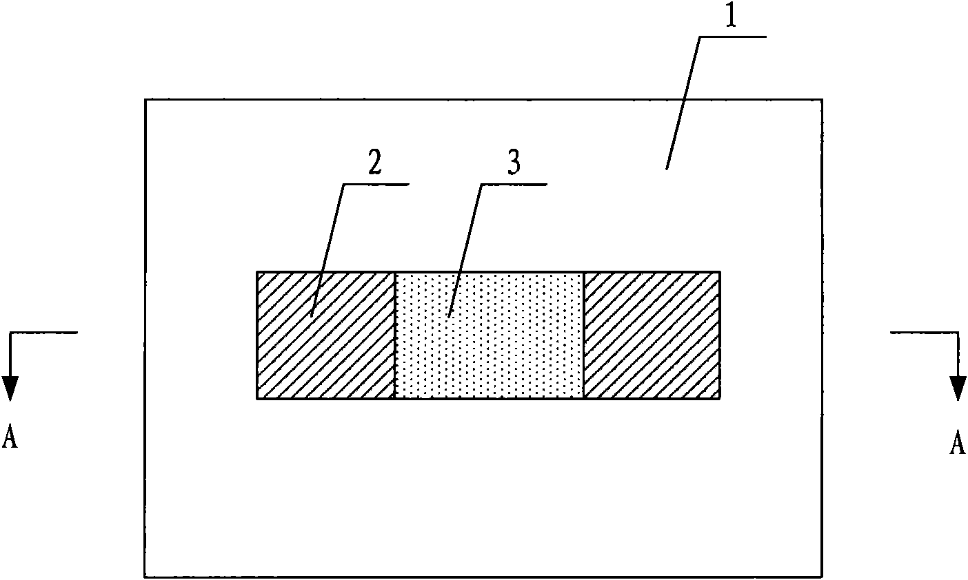
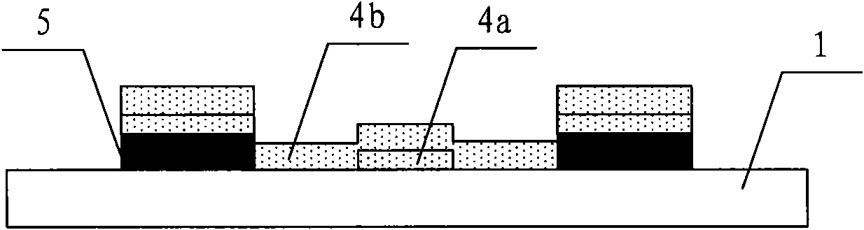
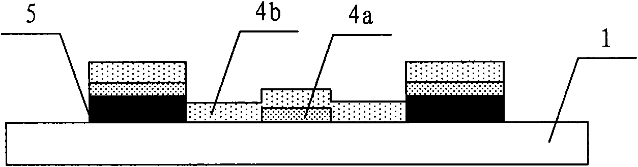
[0074] figure 1 It is a schematic plan view of Embodiment 1 of the mask plate of the present invention, figure 2 for figure 1 Middle A-A sectional view, such as figure 1 , 2 As shown, the mask plate includes a substrate 1. A non-transparent region 2 and a semi-transparent region 3 are formed on the substrate 1. The other regions are completely transparent regions, and a semi-transparent film is arranged in the semi-transparent region 3. The semi-transparent area 3 can be uniformly transparent, and the thickness of the semi-transparent film located in the middle area in the semi-transparent area 3 is greater than the thickness of the semi-transparent film located in the area outside the intermediate area. A metal layer 5 and a semi-permeable film are formed in the non-transparent region 2 . Wherein, the semipermeable membrane includes a first semipermeable membrane 4a and a second semipermeable membrane 4b located on the first semipermeable membrane 4a, and the first se...
PUM
 Abstract
Description
Claims
Application Information