Two-dimensional photonic crystal surface-emitting laser

a photonic crystal surface and laser technology, applied in semiconductor lasers, laser optical resonator construction, laser details, etc., can solve the problems of affecting the operation speed and durability of the laser, and the device is a little bit smaller, so as to achieve the effect of small light loss

Active Publication Date: 2016-12-27
JAPAN SCI & TECH CORP
View PDF15 Cites 12 Cited by
  • Summary
  • Abstract
  • Description
  • Claims
  • Application Information

AI Technical Summary

Benefits of technology

[0049]According to the present invention, it is possible to obtain a two-dimensional photonic crystal surface emitting laser that can emit an inclined beam at a larger inclination angle with a smaller loss in light than that in conventional cases.

Problems solved by technology

However, adding such a scanning mechanism prevents miniaturization of the devices using a semiconductor laser, and works against improvements in their operational speed and durability.

Method used


Image

  • Two-dimensional photonic crystal surface-emitting laser
  • Two-dimensional photonic crystal surface-emitting laser
  • Two-dimensional photonic crystal surface-emitting laser

Examples


first embodiment

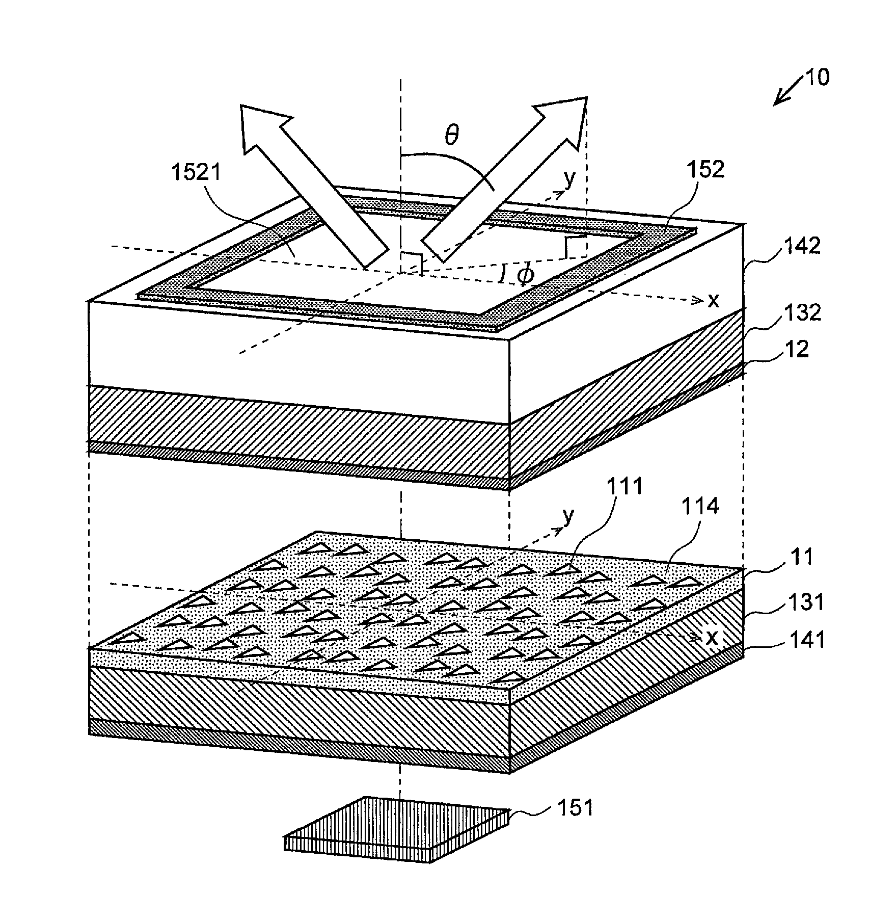
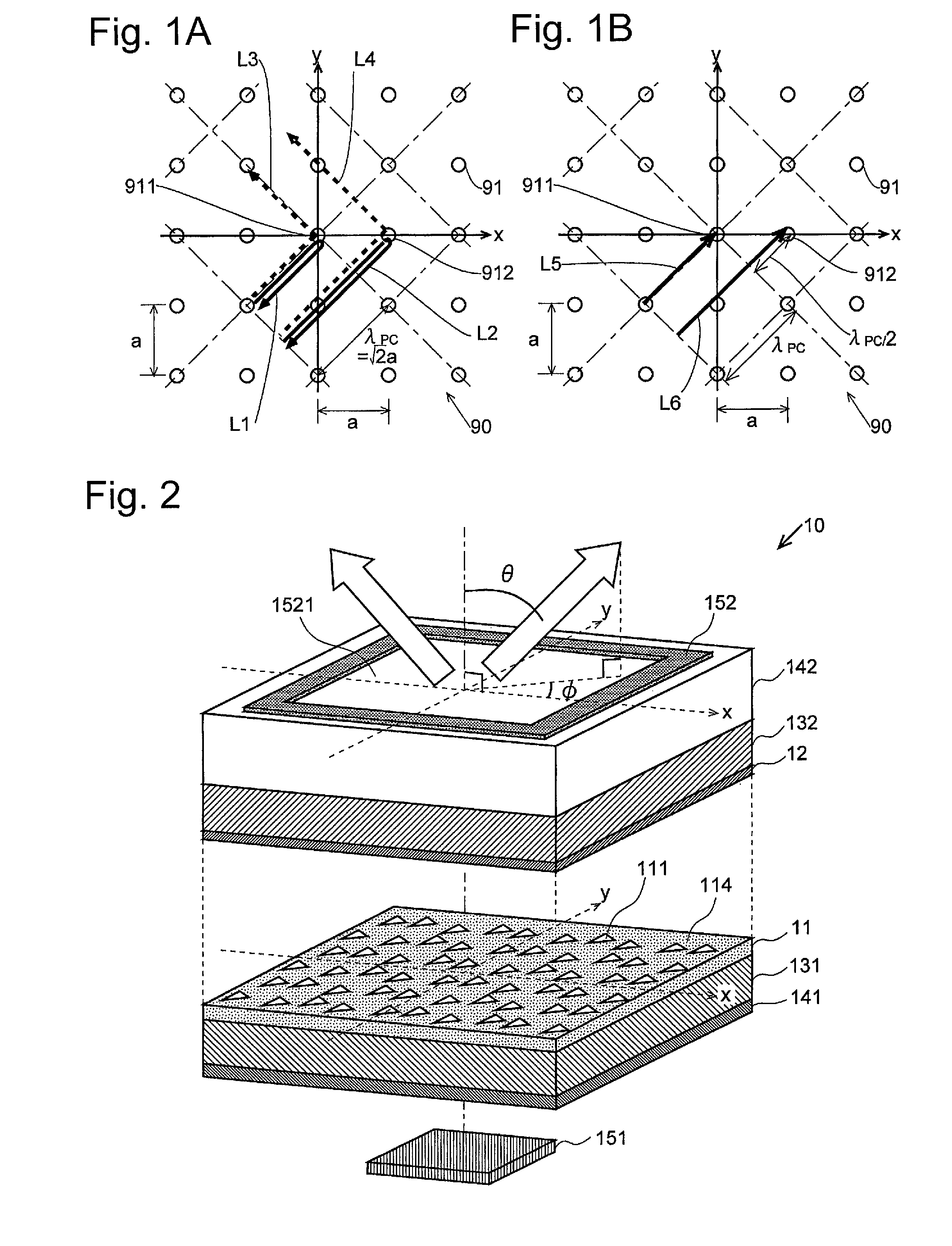
[0067]FIG. 2 is a perspective view of a two-dimensional photonic crystal surface emitting laser (which is hereinafter called the “photonic crystal laser”) 10 of the first embodiment. This photonic crystal laser 10 includes a lower electrode 151, a lower substrate 141, a first cladding layer 131, a two-dimensional photonic crystal layer 11, an active layer 12, a second cladding layer 132, an upper substrate 142, and an upper electrode 152, which are laminated in the stated order. In the photonic crystal laser 10 of the present embodiment, a laser beam is emitted through a window (cavity) 1521 provided in a central part of the upper electrode 152, in a direction inclined by an emission angle θ from the normal to the two-dimensional photonic crystal layer 11. Instead of the electrode including the window 1521, a transparent electrode made of indium tin oxide (ITO) and the like may be used as the upper electrode 152. It should be noted that the two-dimensional photonic crystal layer 11 ...

second embodiment

[0077]Next, an embodiment of a variable beam-direction two-dimensional photonic crystal surface emitting laser (which is hereinafter called the “variable beam-direction photonic crystal laser”) 20 is described as the second embodiment. FIG. 10A is a longitudinal sectional view showing the variable beam-direction photonic crystal laser 20 of the second embodiment. In this embodiment, components similar to those in the photonic crystal laser 10 of the first embodiment are denoted by the same reference signs as those in the first embodiment, and detailed description thereof is omitted. The variable beam-direction photonic crystal laser 20 includes lower electrodes 251, the lower substrate 141, the first cladding layer 131, a two-dimensional photonic crystal layer 21, the active layer 12, the second cladding layer 132, the upper substrate 142, and an upper electrode 252, which are laminated in the stated order. In the present embodiment, a transparent electrode that covers the entire up...

third embodiment

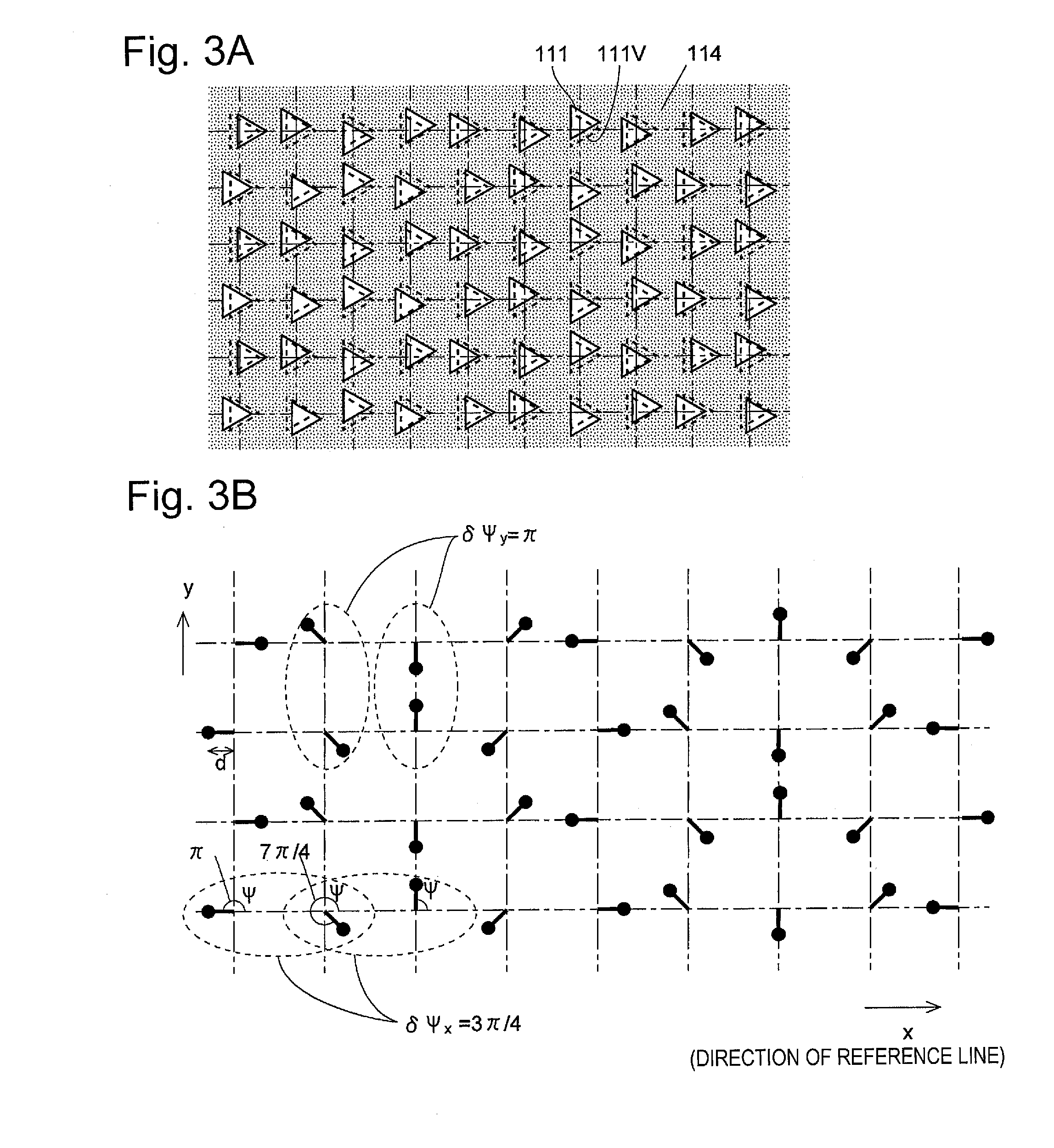
[0085]In the third embodiment, description is given of an example in which: air holes (modified refractive index regions) are shifted in the same direction from lattice points of a basic two-dimensional lattice of a photonic crystal layer; and the distance of the shift is modulated. In the following, because the configuration excluding the photonic crystal layer is similar to that in the first embodiment, description thereof is omitted, and the configuration of the photonic crystal layer is described.

[0086]As shown in FIG. 12A, the basic two-dimensional lattice in the present embodiment is a square lattice similar to that in the first embodiment. The air holes 111 as the modified refractive index regions are respectively arranged at positions shifted from the lattice points of the basic two-dimensional lattice. As shown in FIG. 12B, the direction of the shift is the x direction as a reference direction, for all the air holes 111. Based on the modulation phase Ψ, the distance d of th...


PUM


Abstract

A two-dimensional photonic crystal surface emitting laser has a laminated structure including: a two-dimensional photonic crystal (2DPC) layer in which refractive index distribution is formed by two-dimensionally arranging air holes in a plate-shaped base member; and an active layer for generating light with wavelength λL by receiving an injection of electric current. The two-dimensional photonic crystal surface emitting laser emits a laser beam in the direction of an inclination angle θ from normal to the 2DPC layer.

Description

TECHNICAL FIELD[0001]The present invention relates to a two-dimensional photonic crystal surface emitting laser, and more specifically, to a two-dimensional photonic crystal surface emitting laser that emits a laser beam in a direction inclined from the normal to a crystal surface.BACKGROUND ART[0002]Semiconductor lasers have many advantages, such as small, inexpensive, low power consumption and long service life, and they are used in a wide variety of fields, such as light sources for optical recording, light sources for communication, laser displays, laser printers, and laser pointers. In typical laser displays or laser printers, the laser beam is controlled to scan a certain region so as to form characters or figures. In currently used semiconductor lasers, the scan operation is achieved by controlling the emitting direction of the laser beam by using an additional, external element, such as a polygon mirror, a micro electro-mechanical system (MEMS) micro mirror or an acousto-opt...

Claims


Application Information

Patent Timeline
Patent Type & Authority Patents(United States)
IPC IPC(8): H01S5/00H01S3/10H01S3/00H01S5/042H01S5/18H01S5/10H01S5/185
CPCH01S5/18H01S3/0085H01S3/10H01S5/0425H01S5/105H01S5/1215H01S2301/18H01S5/04256H01S5/04254H01S5/04253H01S5/11H01S5/185
Inventor NODA, SUSUMUOKINO, TSUYOSHIKITAMURA, KYOKOTANAKA, YOSHINORILIANG, YONG
Owner JAPAN SCI & TECH CORP
Why Eureka
Try Eureka