
Quick aligning method and device of integrated photonic device

An integrated photon and fast technology, applied in the coupling of optical waveguide, etc., can solve the problems of poor anti-interference ability, inconvenient operation, large detection area, etc., and achieve the effect of strong anti-interference ability, good detection effect and easy operation

Inactive Publication Date: 2010-02-24
CENT SOUTH UNIV
View PDF0 Cites 14 Cited by
  • Summary
  • Abstract
  • Description
  • Claims
  • Application Information

AI Technical Summary

Problems solved by technology

[0004] ① Large-area infrared detectors: poor anti-interference ability, large detection area, inconvenient operation and generally not used;
[0005] ②IR-CCD (infrared camera): the detection effect is good, but the cost is high

Method used


Image

  • Quick aligning method and device of integrated photonic device
  • Quick aligning method and device of integrated photonic device
  • Quick aligning method and device of integrated photonic device

Examples


Embodiment 1

[0025] Embodiment 1: A method for rapid alignment of an integrated photonic device, characterized by comprising the following steps:

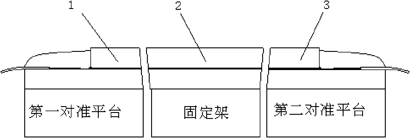
[0026] 1) Fix the first single-mode array fiber on the high-precision first alignment platform with adjustable displacement, the integrated photonic chip on the fixing frame, and the multi-mode array fiber on the high-precision second alignment platform with adjustable displacement On; the first alignment platform and the second alignment platform are respectively arranged on the left and right sides of the fixing frame; by adjusting the first alignment platform and the second alignment platform to complete the single-mode array fiber and integrated photonic chip Best alignment

[0027] 2) Replace the second single-mode array fiber with the multi-mode array fiber and fix it on the second alignment platform, and then use the alignment algorithm to adjust the first alignment platform and the second alignment platform to realize the first single-mode a...


PUM

PropertyMeasurementUnit
Diameteraaaaaaaaaa
Core diameteraaaaaaaaaa

Abstract

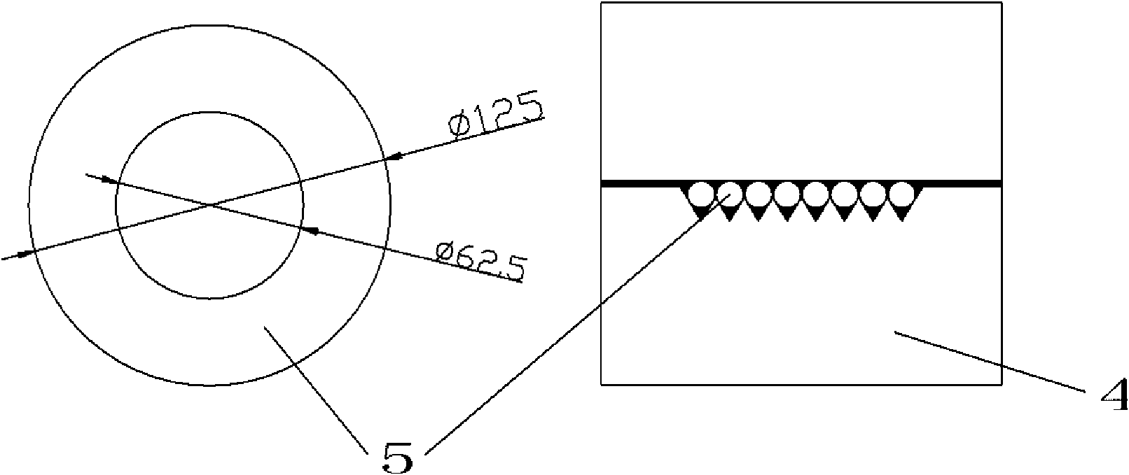
The invention discloses a quick aligning method and a device of an integrated photonic device. The method comprises the following steps: using a multi-mode array optical fiber to carry out initial alignment in the optimal aligning process of a first single mode array optical fiber and an integrated photonic chip; then converting the multi-mode optical fiber into a second single mode array opticalfiber; and carrying out the optimal alignment of the first single mode array optical fiber, the integrated photonic chip and the second single mode array optical fiber by an alignment algorithm. The multi-mode array optical fiber is characterized by using the multi-mode optical fiber with the core diameter of 62.5 microns, and the optical fiber is encapsulated and fixed in a V-shaped groove with aproper specification. The invention has the characteristics of low cost, high efficiency and easy operation and can be generally suitable for the alignment and encapsulation process of the integratedphotonic chip.

Description

Technical field [0001] The invention relates to a method and device for rapid alignment of integrated photonic devices. The method and device are mainly suitable for the alignment and packaging of array optical fibers and integrated photonic chips. Background technique [0002] Integrated photonic devices have outstanding advantages such as compact structure, small size, strong anti-interference ability, good performance consistency, stability and reliability, and ease of automated mass production. In recent years, they have been widely used in optical communication backbone networks and fiber-to-the-home technologies for access networks . In the process of manufacturing integrated photonic devices, the packaging of array fibers and waveguide devices is a very important and critical part, and the packaging cost accounts for 70% to 90% of the total cost, and the packaging time accounts for more than 50% of the total production time. So a stable and fast packaging method will make...

Claims


Application Information

Patent Timeline
IPC IPC(8): G02B6/26
Inventor 段吉安郑煜阳波徐洲龙李罡
Owner CENT SOUTH UNIV
Learn More