
Spacer used between liquid crystal substrates and packaging structure with same
A technology of liquid crystal substrate and packaging structure, applied in the field of gasket structure, can solve the problems of crushing the lower substrate, sticking liquid crystal substrate, mechanical failure, etc., and achieves the effect of improving the sticking problem and reducing the crushing of the lower layer.
- Summary
- Abstract
- Description
- Claims
- Application Information
AI Technical Summary
Problems solved by technology
Method used
Image

Examples
Embodiment Construction
[0018] The specific implementation manners of the present invention will be described in further detail below with reference to the accompanying drawings.
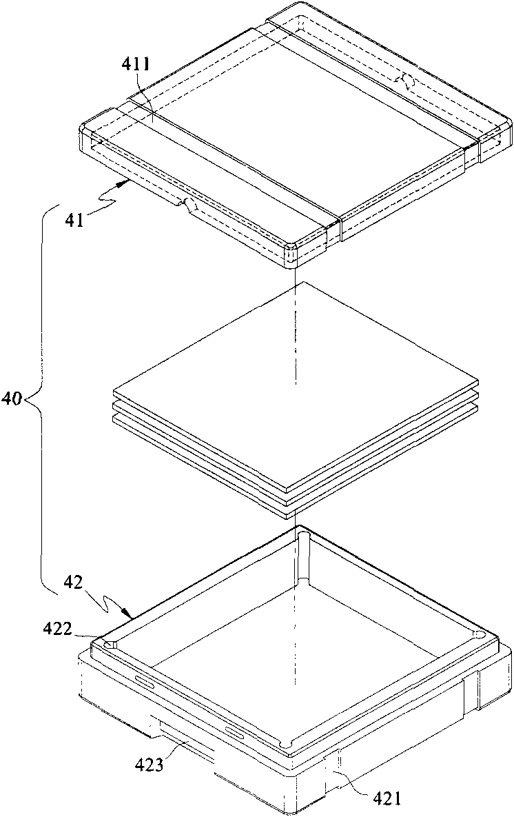
[0019] figure 1 A schematic diagram of a buffer element used between liquid crystal substrates in the prior art is shown. refer to figure 1 , the packaging structure includes: a substrate pair 40 with an upper substrate 41 and a lower substrate 42 , a plurality of grooves 411 on the substrate 41 , positioning holes 422 on the substrate 42 and concave portions 421 and 423 . Wherein, between the upper substrate 41 and the lower substrate 42, a planar buffer element made of polymer material is interposed. In addition, the outer edge of the polymer buffer element is connected to the glass substrate to absorb the force acting on the glass substrate due to external vibrations, thereby reducing packaging costs and preventing damage to the glass substrate without damaging the glass substrate. The short-circuit failure of the ci...
PUM
 Abstract
Description
Claims
Application Information