TFT-LCD array substrate structure and preparation method thereof

An array substrate structure and substrate technology, which is applied in semiconductor/solid-state device manufacturing, semiconductor/solid-state device components, instruments, etc., can solve the problem of reducing the aperture ratio of TFT-LCD, reducing the aperture ratio of TFT-LCD, and reducing the effectiveness of array substrates. Display area and other issues to achieve the effect of increasing the aperture ratio, improving product performance, and reducing signal delay

Active Publication Date: 2010-03-03
K TRONICS (SUZHOU) TECH CO LTD +1
View PDF0 Cites 17 Cited by
  • Summary
  • Abstract
  • Description
  • Claims
  • Application Information

AI Technical Summary

Problems solved by technology

[0004] However, the inventor found in the process of realizing the present invention that although increasing the cross-sectional width of the gate lines or data lines in the array substrate along the width direction in the prior art can alleviate the signal delay, when the area of ​​the array substrate is the same, increasing the gate line or data line The cross-sectional width of the line along the width direction will reduce the effective display area of ​​the array substrate, resulting in a decrease in the aperture ratio (Aperture Ratio) of the TFT-LCD.
It can be seen that at least there are technical defects such as reducing the aperture ratio of TFT-LCD in the prior art

Method used


Image

  • TFT-LCD array substrate structure and preparation method thereof
  • TFT-LCD array substrate structure and preparation method thereof
  • TFT-LCD array substrate structure and preparation method thereof

Examples


Embodiment Construction

[0056] The technical solutions of the present invention will be described in further detail below with reference to the accompanying drawings and embodiments.

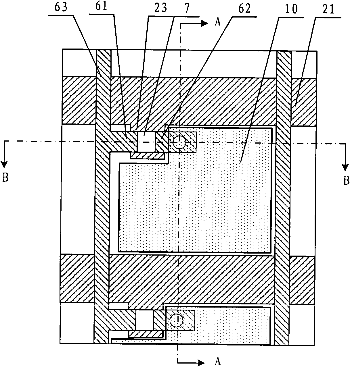
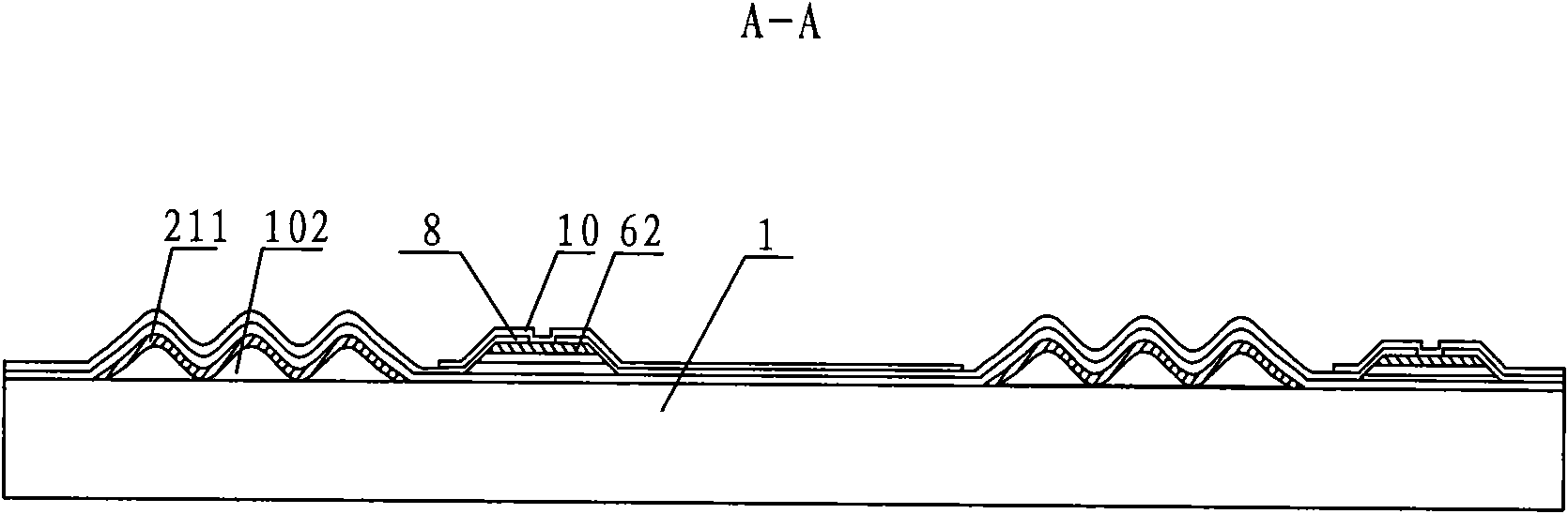
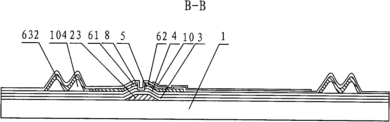
[0057] In each of the following detailed embodiments, the normal grid line or normal data line is the grid line or data line formed by the existing TFT-LCD array substrate structure preparation method, and the shape of the cross section of the grid line or data line is a rectangle; Shaped grid lines or wavy data lines are new grid lines or new data lines that can be formed by the improved TFT-LCD array substrate structure preparation method of the present invention, and the new grid lines or new data lines are formed on the wavy base of the substrate , the cross-sectional shape of the wavy base along the width direction is wavy; the cross-sectional shape of the new grid line or new data line formed on the wavy base along the width direction is an undulating curve similar to waves, that is, wavy.

[0058] Figure 1a It ...


PUM

PropertyMeasurementUnit
heightaaaaaaaaaa

Abstract

The invention relates to a TFT-LCD array substrate structure and a preparation method thereof. The TFT-LCD array substrate structure comprises gate lines and data lines which define a pixel area; thinfilm transistors are formed at crossing positions of the gate lines and the data lines, and are connected with pixel electrodes formed in the pixel area; waved bases used for forming the gate lines and/or the data lines are formed between the gate lines or the data lines and a substrate; the shape of the cross section of each waved base along the width direction is waved; and the gate lines and/or data lines formed on the waved bases are waved gate lines and/or waved data lines. The TFT-LCD array substrate structure can reduce the line resistance of the gate lines and/or the data lines, is favorable for reducing signal delay, and cannot reduce the aperture ratio of a TFT-LCD; or the aperture ratio of the TFT-LCD can be increased to improve product performance while the critical dimensionof the gate lines or the data lines is maintained.

Description

technical field [0001] The invention relates to the field of display, in particular to a thin film transistor liquid crystal display (ThinFilm Transistor Liquid Crystal Display, TFT-LCD for short) array substrate structure and a preparation method thereof. Background technique [0002] Thin film transistor liquid crystal display (TFT-LCD) has the characteristics of small size, low power consumption, and no radiation, and occupies a dominant position in the current flat panel display market. For TFT-LCD, the array substrate (Array) structure and manufacturing process have an important impact on product performance. Among them, parameters such as signal delay (RC Delay) and aperture ratio (Aperture Ratio) of the oscillation circuit are important to measure product performance. parameter. In order to meet the market demand, large-size display is one of the development trends of TFT-LCD; and large-size TFT-LCD puts forward higher requirements on various performance indicators o...

Claims


Application Information

Patent Timeline
Patent Type & Authority Applications(China)
IPC IPC(8): H01L27/12H01L23/522H01L21/84H01L21/768G02F1/1362
Inventor 郝昭慧
Owner K TRONICS (SUZHOU) TECH CO LTD
Why Eureka
Try Eureka