Surface form deviation measurement method of flat optical element

An optical element and surface deviation technology, which is applied in the field of surface deviation measurement of flat optical components, can solve the problems of large influence of measurement results, cumbersome process, low measurement accuracy, etc., to reduce manual participation, improve measurement accuracy, and reduce detection. cost effect

Inactive Publication Date: 2010-03-17
SHANGHAI SECOND POLYTECHNIC UNIVERSITY
View PDF0 Cites 6 Cited by
  • Summary
  • Abstract
  • Description
  • Claims
  • Application Information

AI Technical Summary

Problems solved by technology

At present, the manual drawing method can meet the low-cost inspection requirements of the optical component production workshop, but the process is cumbersome and the measurement accuracy is not high
As people's processing requirements for planar optical components are getting higher and higher, this method can no longer meet the requirements of high precision, strong adaptability and automatic measurement.
Although the surface deviation of planar optical elements can be obtained by visual interpretation method, the disadvantage of this method is that the measurement results obtained are greatly affected by different visual interpretation readers. The interpretation results of the
This brings difficulties to the high-precision processing of optical components in the actual production process

Method used


Image

  • Surface form deviation measurement method of flat optical element
  • Surface form deviation measurement method of flat optical element
  • Surface form deviation measurement method of flat optical element

Examples


Embodiment Construction

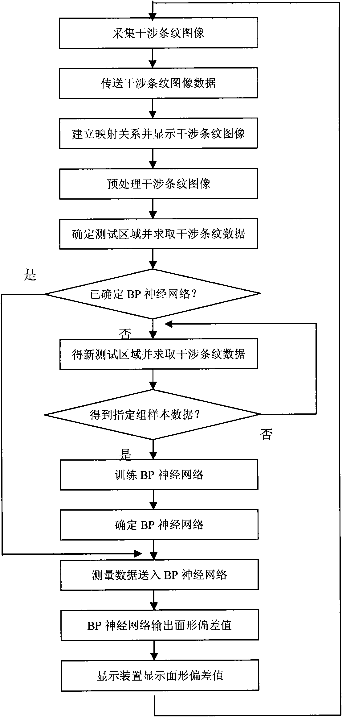
[0032] Below in conjunction with accompanying drawing and embodiment the present invention is described in further detail, but present embodiment is not intended to limit the present invention, and every adopt similar structure of the present invention, method and similar variation thereof, all should be included in the protection scope of the present invention.

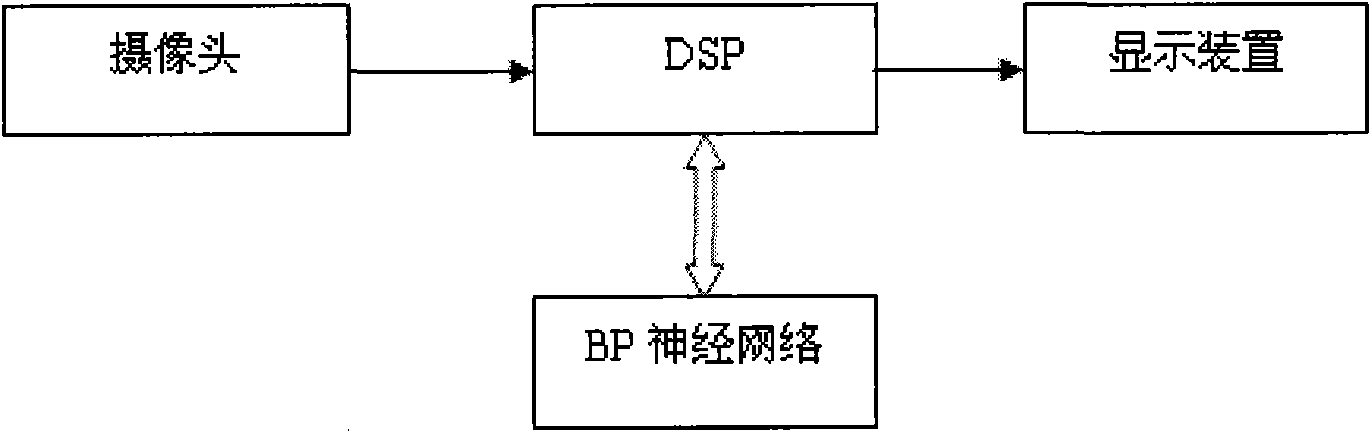
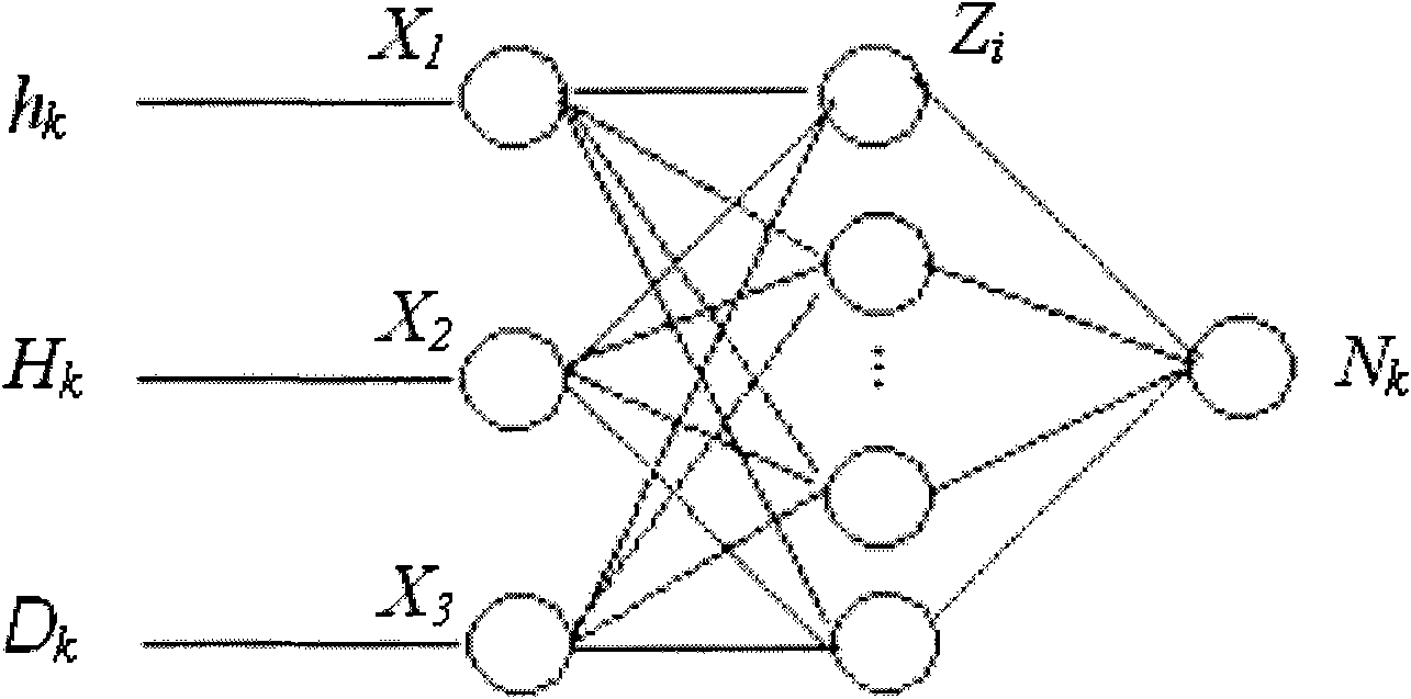
[0033] figure 1 It is a system block diagram of a surface deviation measuring system adopting the measuring method of the present invention. It can be seen from the figure that the surface shape deviation measurement system of the present invention includes: a camera, a digital signal processor (DSP), a BP neural network and a display device.

[0034] The pixel of the camera is 320×240; the DSP adopts TMS320DM642. The display device includes a color graphic dot-matrix liquid crystal display and a monochrome graphic dot-matrix liquid crystal display, and the display device is used to display the processed interferenc...


PUM


Abstract

The invention discloses a surface form deviation measurement method of a flat optical element. Firstly, a camera collects a standard sample image data and sends the collected standard sample image data to DSP via a USB interface for digital signal processing; the processed image data trains a BP neural network to determine the adopted BP neural network; because the camera collects the interferencefringe image data of a measured flat optical element, the camera sends the collected image data to the DSP via the USB interface for digital signal processing, and the obtained measuring data is sentto a determined BP neural network for calculation; the BP neural network outputs a surface form deviation value and sends into a DSP cache region; and the DSP sends the surface form deviation value to a display device for displaying. Because a manipulator can conveniently observe the interference fringe image and adjust the light path, detection cost is lowered; the measuring result is not affected by a person of visual interpretation, thus effectively improving measurement precision.

Description

technical field [0001] The invention relates to a method for measuring surface deviation of a planar optical element. Background technique [0002] The surface deviation of the planar optical element can be obtained by processing the interference fringe image, and the surface deviation value reflects the surface processing information of the measured planar optical element. How to detect the surface deviation of planar optical elements accurately, conveniently and at low cost plays an important role in improving the high-precision processing of planar optical elements. At present, the manual drawing method can meet the low-cost inspection requirements of the optical component production workshop, but the process is cumbersome and the measurement accuracy is not high. As people have higher and higher requirements for the processing of planar optical components, this method can no longer meet the requirements of high precision, strong adaptability and automatic measurement. ...

Claims


Application Information

Patent Timeline
IPC IPC(8): G01B11/24G06N3/02G06N3/08
Inventor 江晓军刘正国
Owner SHANGHAI SECOND POLYTECHNIC UNIVERSITY
Why Eureka
Try Eureka