Solar photovoltaic electrochromic device
An electrochromic device and electrochromic technology, applied in photovoltaic power generation, electrical components, semiconductor devices, etc., can solve the problems of lower transmittance of silicon thin-film solar cells, iris effect, etc., to reduce demand for power generation and increase transmittance , reducing the effect of constituent materials or thickness
- Summary
- Abstract
- Description
- Claims
- Application Information
AI Technical Summary
Problems solved by technology
Method used
Image

Examples
experiment example 1
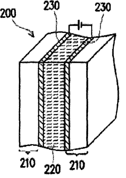
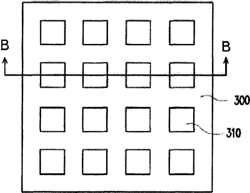
[0081] Prepare the transparent glass substrate first. In addition, 0.05 grams of lithium perchlorate and 0.05 grams of methyl viologen (1,1'-dimethyl-4,4'-bipyridinium dichloride, 1,1'-dimethyl-4,4'-bipyridinium dichloride compound) was dissolved in 5 milliliters of pure water and stirred to form a uniform, transparent and colorless electrochromic solution. The electrochromic solution was coated on the above-mentioned transparent glass substrate, and then the translucent thin-film solar cell substrate with an area of 15 cm×15 cm was attached to the transparent glass substrate with epoxy glue. Among them, silicon thin film solar cells are used, and the silicon thin film solar cells are arranged in a matrix, and the area of a single matrix is about 0.25cm 2 . The thickness of the above-mentioned epoxy resin glue is about 0.5 cm, and glass balls are mixed therein as spacers to make a certain distance between the two base materials.
[0082] Among them, the semi-transpare...
experiment example 2
[0085] Prepare the transparent glass substrate first. In addition, 0.05 g of 5,10-dihydro-5,10-dimethylphenazine (5,10-dihydro-5,10-dimethylphenazine) was dissolved in 5 ml of propylene carbonate (propylenecarbonate) solvent, and stirred Dubbed into a uniform, transparent and colorless electrochromic solution. The electrochromic solution was coated on the above-mentioned transparent glass substrate, and then the translucent thin-film solar cell substrate with an area of 15 cm×15 cm was attached to the transparent glass substrate with epoxy glue. Among them, silicon thin film solar cells arranged in a matrix are used, and the area of a single matrix is about 0.25cm 2 , its structure is the same as in Example 1. The thickness of the above-mentioned epoxy resin glue is about 0.5 cm, and glass balls are mixed therein as spacers to make a certain distance between the two base materials.
[0086] The open circuit voltage Voc of the semi-transparent thin film solar cell is 0...
PUM
| Property | Measurement | Unit |
|---|---|---|
| thickness | aaaaa | aaaaa |
| thickness | aaaaa | aaaaa |
| current density | aaaaa | aaaaa |
Abstract
Description
Claims
Application Information
 - R&D
- Intellectual Property
- Life Sciences
- Materials
- Tech Scout
- Unparalleled Data Quality
- Higher Quality Content
- 60% Fewer Hallucinations
Browse by: Latest US Patents, China's latest patents, Technical Efficacy Thesaurus, Application Domain, Technology Topic, Popular Technical Reports.
© 2025 PatSnap. All rights reserved.Legal|Privacy policy|Modern Slavery Act Transparency Statement|Sitemap|About US| Contact US: help@patsnap.com