Model and method for measuring resistance of contact holes or through holes in bipolar transistor components

A bipolar transistor and measurement model technology, which is applied in semiconductor/solid-state device testing/measurement, electric solid-state devices, semiconductor devices, etc., can solve problems such as large errors and inability to accurately measure the resistance value of the contact layer

Active Publication Date: 2010-03-17
SHANGHAI HUAHONG GRACE SEMICON MFG CORP
View PDF0 Cites 17 Cited by
  • Summary
  • Abstract
  • Description
  • Claims
  • Application Information

AI Technical Summary

Problems solved by technology

[0009] This calculation method can only roughly measure and calculate a single contact hole or through hole. When the resistance value of the contact hole or through hole is small, the error of this measurement method is relatively large, and the specific contact cannot be accurately measured. layer resistance

Method used


Image

  • Model and method for measuring resistance of contact holes or through holes in bipolar transistor components
  • Model and method for measuring resistance of contact holes or through holes in bipolar transistor components
  • Model and method for measuring resistance of contact holes or through holes in bipolar transistor components

Examples


Embodiment Construction

[0027] In order to better understand the technical content of the present invention, specific embodiments are given together with the attached drawings for description as follows.

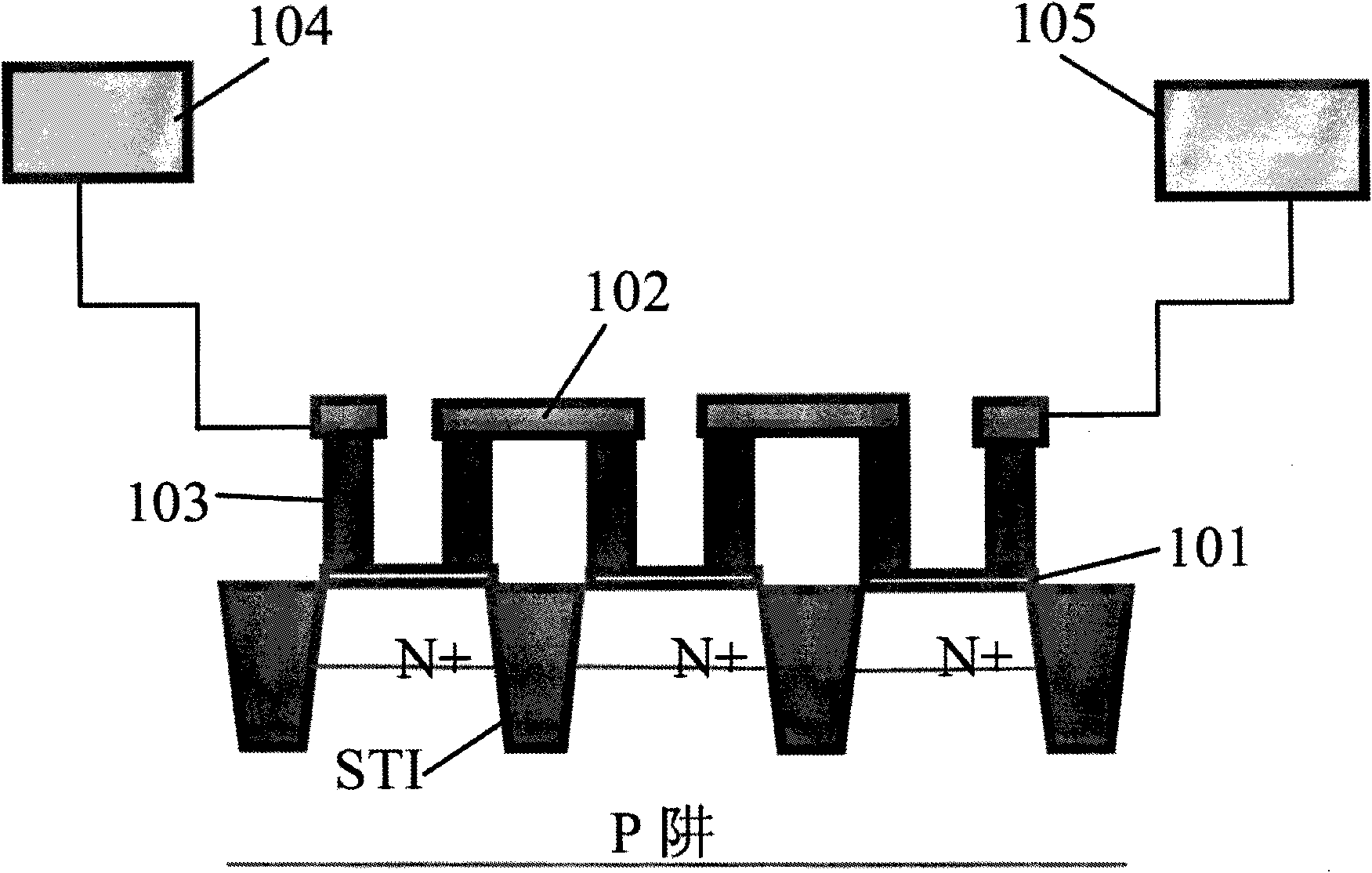
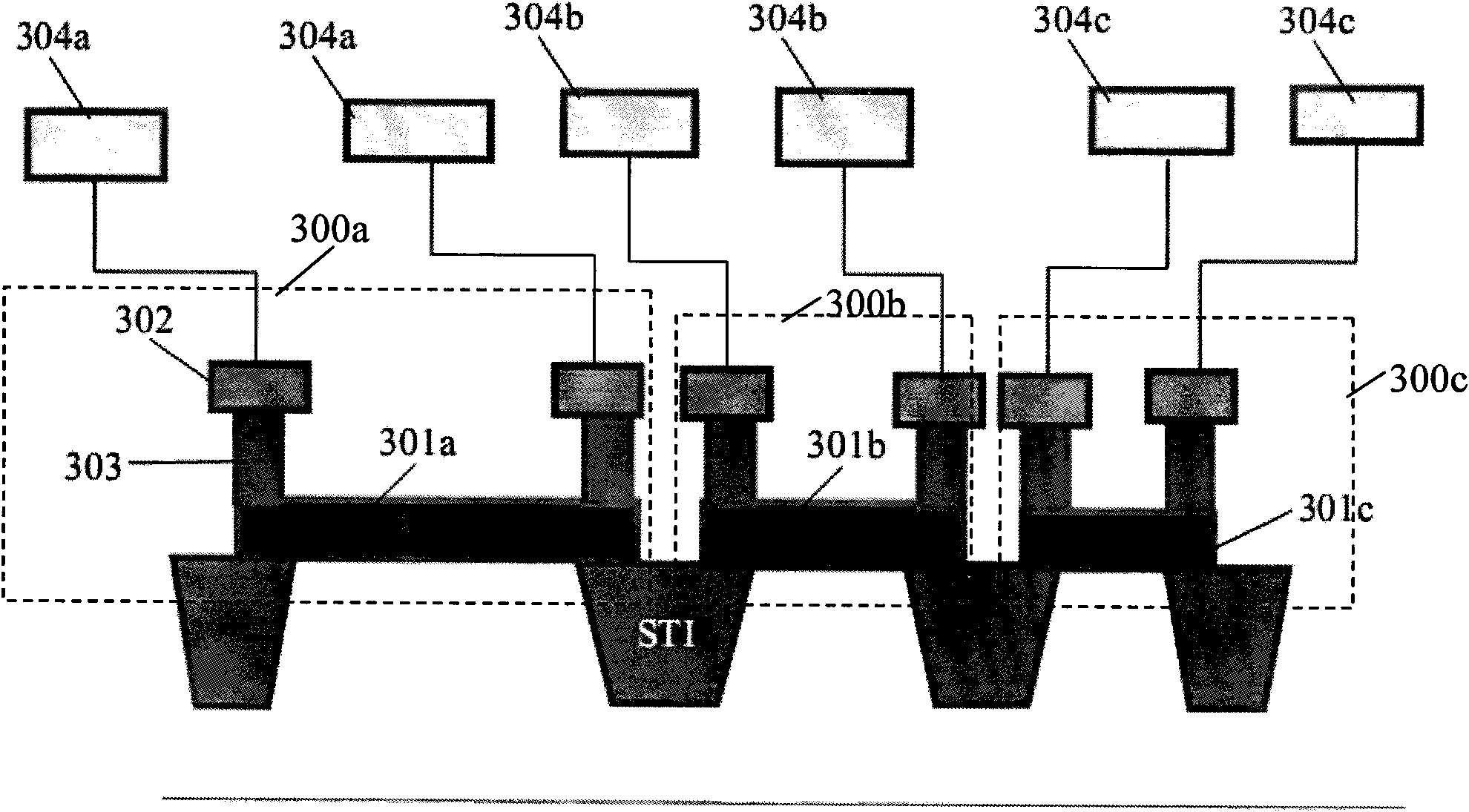
[0028] image 3 Shown is a measurement model for measuring the resistance value of a contact hole in a preferred embodiment of the present invention.

[0029] Different from the method of measuring the total resistance value flowing through a plurality of contact holes and then averaging in the prior art, this embodiment measures the resistance of resistance devices with different widths (W) and lengths (L) multiple times, and fits the corresponding curves, The intercept of the curve is the resistance of the contact hole.

[0030] image 3 Other structures of the medium-resistance device, such as P-well, STI isolation, etc., will not be described here one by one. In this embodiment, a plurality of resistance devices 300a-300c are included, and each resistance device 300a-300c includes polysilico...


PUM


Abstract

The invention provides a model and a method for measuring the resistance of contact holes or through holes in bipolar transistor components, used for measuring the resistance of contact holes and through holes in the back-end process of transistor components. The model consists of a plurality of resistor components, wherein, a group of poly-silicon resistors or diffused resistors with different lengths and widths are required to be designed for measuring the resistance of the contact holes; and a group of metal resistors with different lengths and widths are required to be designed for measuring the resistance of the through holes. Each poly-silicon resistor consists of a poly-silicon layer, a contact hole and metal lead-out; each diffused resistor consists of an N-type or P-type diffusedlayer, a contact hole and metal lead-out, wherein, the contact hole is located between the poly-silicon layer or the diffused layer and the metal layer and used for leading out the poly-silicon resistors or the diffused resistors; and each metal resistor consists of a certain layer of metal, a through hole and metal lead-out, wherein, the through hole is located between two layers of metal and used for leading out the metal resistors in the lower layer. The current passing the resistors can be measured by applying voltage to two resistor lead-out ends of each resistor.

Description

technical field [0001] The invention relates to a measurement model and method for measuring resistance, and more particularly relates to a measurement model and method for measuring a contact hole or a through hole in a bipolar transistor of a SiGe process. Background technique [0002] In the transistor process, contact holes (contacts) and vias (vias) are required for the extraction of devices. Contact holes and via holes are the connection parts between different layers. area) and metal (metal), and through holes are between metal and metal. [0003] During the fabrication of transistors in the SiGe process, it is necessary to monitor the resistance of the contact holes or vias. Existing measurement models for measuring contact hole or via resistance are as follows: figure 1 and figure 2 shown. [0004] figure 1 Shown is a measurement model for measuring contact hole resistance in the prior art. The measurement model includes N+ / P+ diffused region silicide resista...

Claims


Application Information

Patent Timeline
Patent Type & Authority Applications(China)
IPC IPC(8): H01L23/544H01L23/52H01L21/66
Inventor 王兵冰许丹
Owner SHANGHAI HUAHONG GRACE SEMICON MFG CORP
Why Eureka
Try Eureka