

Circuit simulation based on gate spacing from adjacent mos transistors
一种MOS晶体管、电路仿真的技术,应用在电数字数据处理、特殊数据处理应用、仪器等方向,能够解决影响晶体管漏电流、不足电路仿真等问题,达到提高精确度的效果
- Summary
- Abstract
- Description
- Claims
- Application Information
AI Technical Summary
Problems solved by technology
Method used
Image

Examples
Embodiment Construction
[0038] The invention will now be described herein with reference to illustrated embodiments. Those skilled in the art will appreciate that many alternative embodiments can be accomplished using the teachings of the present invention and that the invention is not limited to the embodiments illustrated for explanatory purposes.
[0039] 1. The concept of circuit simulation technology
[0040] First, refer to figure 1 , to describe the concept of circuit simulation technology in one embodiment of the present invention.
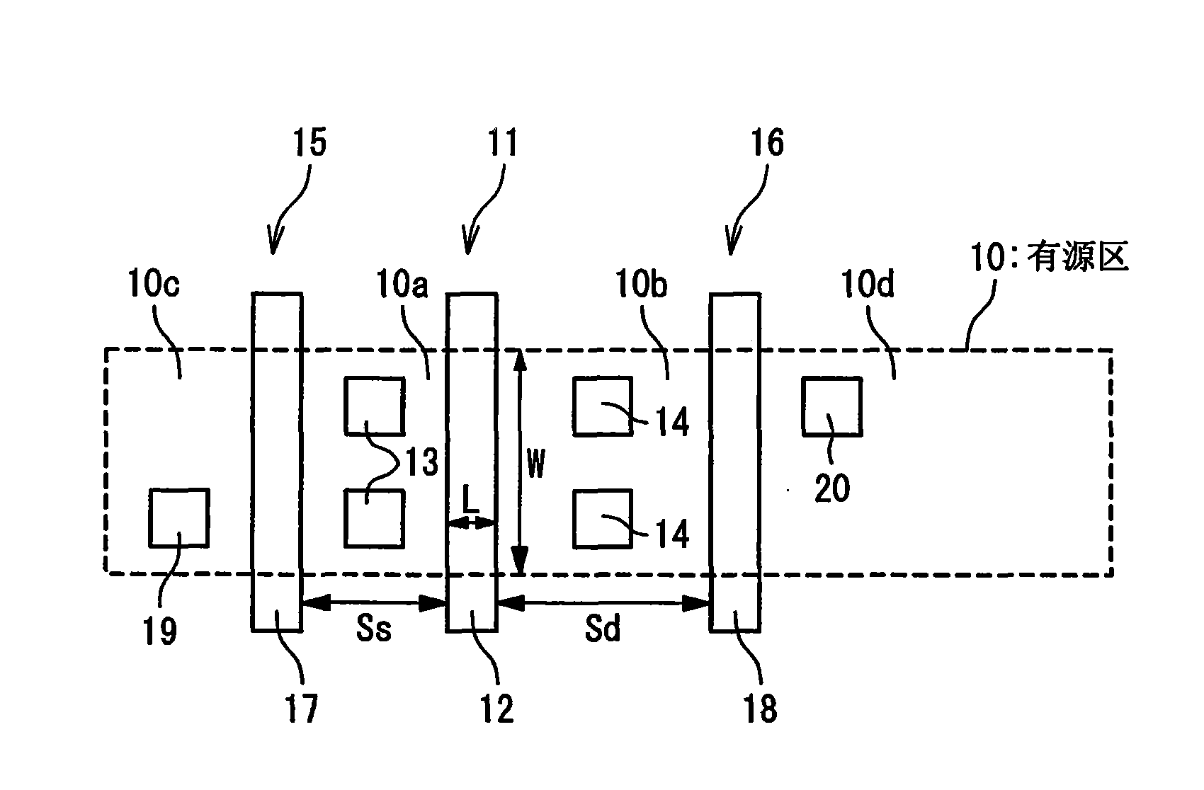
[0041] figure 1 is a diagram showing an example of the layout of an integrated circuit to be simulated. exist figure 1In , reference numeral 10 denotes an active region and reference numeral 11 denotes a MOS transistor to be simulated (hereinafter referred to as "target transistor"). Reference numeral 12 denotes a gate of the MOS transistor 11 . A gate 12 is provided across the active region 10 . A region directly under gate 12 in active region 10 serves...
PUM
 Abstract
Description
Claims
Application Information