Multilayer circuit board, manufacture method thereof and communication equipment

A multi-layer circuit board and communication equipment technology, applied in multi-layer circuit manufacturing, printed circuit manufacturing, circuits, etc., can solve problems such as increasing process flow and affecting production efficiency

Inactive Publication Date: 2010-03-31
HUAWEI TECH CO LTD
View PDF0 Cites 62 Cited by
  • Summary
  • Abstract
  • Description
  • Claims
  • Application Information

AI Technical Summary

Problems solved by technology

[0005] Partial metal substrates need to be assembled separately, which increases t

Method used


Image

  • Multilayer circuit board, manufacture method thereof and communication equipment
  • Multilayer circuit board, manufacture method thereof and communication equipment
  • Multilayer circuit board, manufacture method thereof and communication equipment

Examples


Embodiment Construction

[0029] The following will clearly and completely describe the technical solutions in the embodiments of the present invention with reference to the accompanying drawings in the embodiments of the present invention. Obviously, the described embodiments are only some, not all, embodiments of the present invention. Based on the embodiments of the present invention, all other embodiments obtained by persons of ordinary skill in the art without creative efforts fall within the protection scope of the present invention.

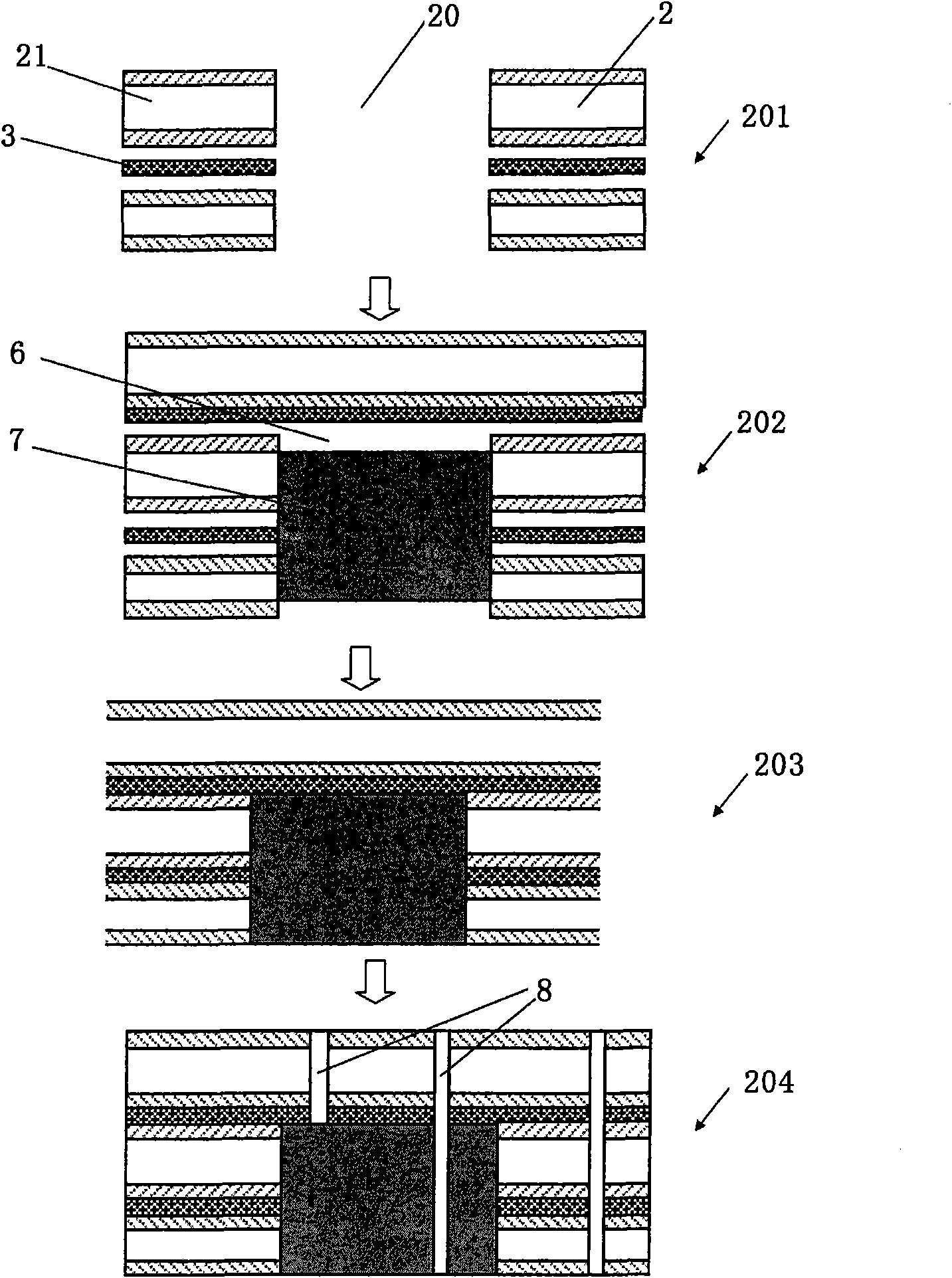
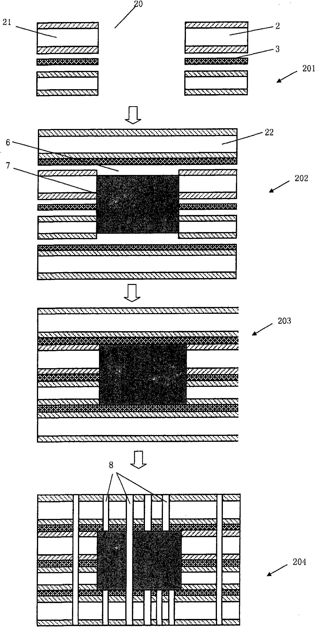
[0030] Such as figure 2 or image 3 As shown, the present invention provides an embodiment of a method for making a multilayer circuit board, comprising:

[0031] Step 201, opening at least one sub-board 2 with a stage slot 20 to form a first sub-board 21;

[0032] Step 202, stacking at least one sub-board 2 and the dielectric layer 3 together, wherein the sub-board 2 includes the first sub-board 21, and the first sub-board 21 makes the set stage groove 20 Plac...


PUM


Abstract

The embodiment of the invention discloses a multilayer circuit board, a manufacture method thereof and communication equipment. The multilayer circuit board comprises at least one sub-board which is provided with step grooves to form a first sub-board and is stacked together with a dielectric layer, wherein the sub-board comprises the first sub-board; the first sub-board is placed in the mode of communicating the step grooves; a holding groove is formed after the step grooves are communicated; a heat-conducting block is placed in the holding groove; the dielectric layer is positioned between the sub-boards; the sub-boards stacked together, the dielectric layer and the heat-conducting block are pressed; and the sub-boards and the heat-conducting block which are pressed together are made into the multilayer circuit board. The process of assembling the heat-conducting block is simplified by embedding the heat-conducting block when the circuit board is pressed.

Description

technical field [0001] The invention relates to the technical field of electronic communication, in particular to a multilayer circuit board, a manufacturing method thereof and communication equipment. Background technique [0002] With the vigorous development of the electronics industry, circuit boards are used more and more widely, and electronic devices are mostly assembled on circuit boards for operation, such as: power tubes, QFN (quad flat non-leaded package, four-sided non-pin flat package) , BGA (ball grid array, spherical contact display), CSP (chip scalepackage, chip size package), QFP (quad flat package, four-side pin flat package), etc., with the increasing number of electronic devices on the circuit board, heat dissipation Questions become more and more important. [0003] For electronic devices with high power, at present, the method of partially embedding metal substrates on the circuit board is mostly used to dissipate heat from the electronic devices. [...

Claims


Application Information

Patent Timeline
IPC IPC(8): H05K3/46H05K7/20H01L21/48H01L23/498H01L23/367
CPCH05K2201/09309H05K2203/063H05K1/0204H05K2201/10416H05K1/0206H05K3/4611H05K1/0201H05K3/4614Y10T29/49124H05K2201/09554H05K3/4038
Inventor 黄明利张顺杨曦晨赵俊英罗兵李志海汪国亮
Owner HUAWEI TECH CO LTD
Why Eureka
Try Eureka