Module board having embedded chips and components and method of forming the same

Inactive Publication Date: 2005-06-09
VIA TECH INC
View PDF10 Cites 52 Cited by
  • Summary
  • Abstract
  • Description
  • Claims
  • Application Information

AI Technical Summary

Benefits of technology

[0012] It is another object of the invention to decrease the process costs.
[0013] Yet another object of the invention is to make the electrical test more convenient.
[0014] It is a further object of the invention to control the thickne

Problems solved by technology

First, the packaging of IC chips, the assembly of passive components' surface mount technology (SMT) must proceed individually, resulting in a lengthy procedure, low yield, and high product costs.
Second, since the assembly of passive components and the SMT cannot be integrated at the same packaging level, it is impossible to reduce the product to a desired thickness.
Third, in order to achieve heat dissipation, a heat sink/fan

Method used


Image

  • Module board having embedded chips and components and method of forming the same
  • Module board having embedded chips and components and method of forming the same
  • Module board having embedded chips and components and method of forming the same

Examples


Embodiment Construction

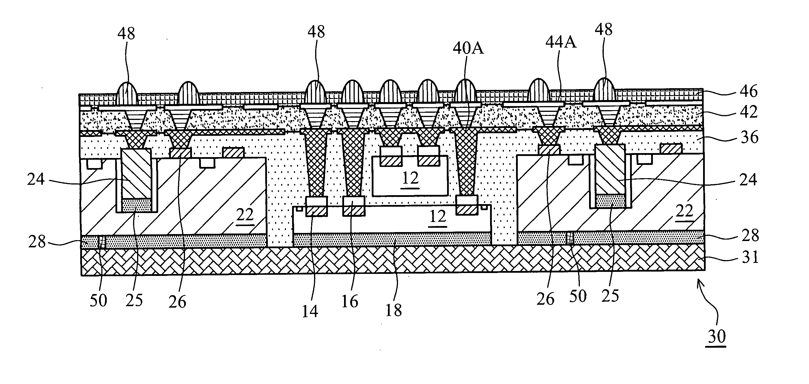
[0021] The present invention provides a module board, similar to a cavity-down plastic ball grid array (CD-PBGA) substrate or a substrate having various cavities, constituting a substrate having cavities and a heat-dissipation sheet adhering to each other. A plurality of passive components (or integrated passive module) and IC chips are formed in the cavities of the substrate. A multi-layered interconnection process can directly proceed on the module board to provide electrical connection to other circuit boards in a cavity down manner. In accordance with the number of the IC chips and variations in the packaging process, the module board may serve as a module component, a multi-chip module (MCM) substrate or a main board to be applied to every fabricating level in the electrical packaging technology.

[0022] FIGS. 1 to 9 are sectional diagrams showing a method of forming the module board according to the present invention.

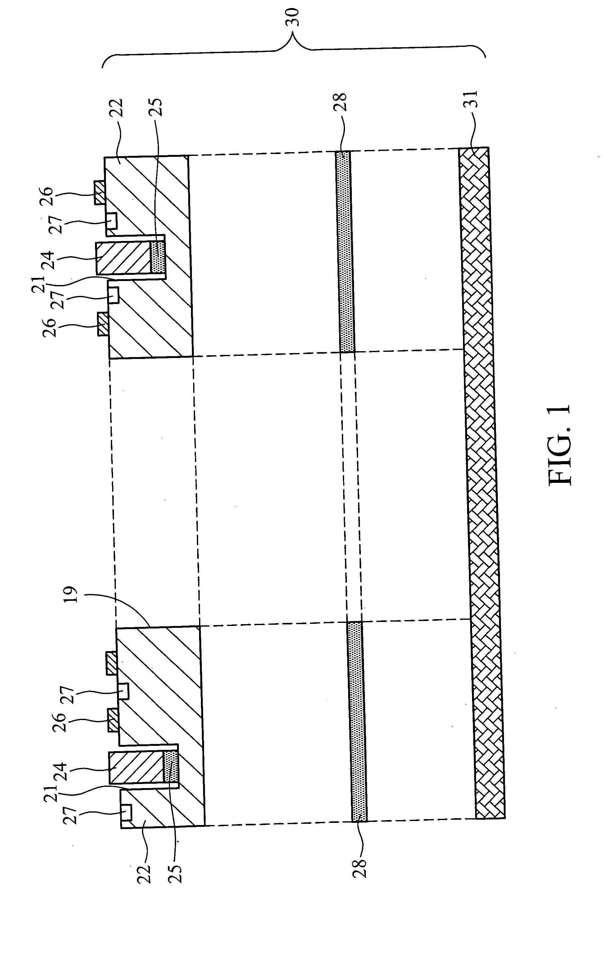
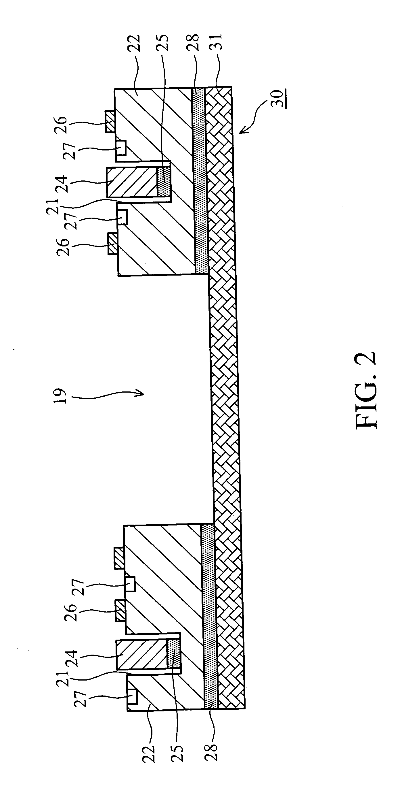
[0023] As shown in FIG. 1, a substrate 22, a first adhesion ...


PUM


Abstract

A module board has embedded chips and components. A substrate has at least one large cavity and at least one small cavity, in which the large cavity passes through the substrate and a passive component is set in the small cavity. A heat-dissipation sheet is set at the bottom of the substrate. A first adhesion layer bonds the bottom of the substrate to the heat-dissipation sheet. At least one IC chip is fixed in the large cavity of the substrate by a second adhesion layer. A dielectric filling layer covers the entire surface of the module board and fills all gaps, in which the dielectric filling layer has a plurality of micro vias to expose partial areas of the IC chip, the passive component and the substrate. At least one wiring pattern layer is formed on the dielectric filling layer and provide electrical connection among the IC chip, the passive component, and the substrate.

Description

[0001] This application is a continuation-in-part of application Ser. No. 10 / 431,458 filed on May 8, 2003, now pending.BACKGROUND OF THE INVENTION [0002] 1. Field of the Invention [0003] The present invention relates to a module board and a method of forming the same. More particularly, the present invention relates to an integrated module board, with a structure similar to a cavity-down plastic ball grid array (CD-PBGA) substrate or a substrate having various cavities, in which all kinds of chips and components are embedded or mounted onto the module board. [0004] 2. Description of the Related Art [0005] Electrical packaging, including attachment of IC chips, electrical connections of circuits, sealing, assembly of a circuit board, system integration and product packing, integrates IC chips with essential components to achieve electric communication, circuit-signal communication, heat-dissipation path, loading capability and protection. In general, electrical packaging technology i...

Claims


Application Information

Patent Timeline
IPC IPC(8): H01L23/538H05K1/18
CPCH01L23/5389H01L2924/19105H01L24/82H01L2223/5448H01L2223/54486H01L2224/24227H01L2224/82039H01L2924/01029H01L2924/01078H01L2924/01079H01L2924/01082H01L2924/14H01L2924/15153H01L2924/1517H01L2924/15311H01L2924/19041H01L2924/19043H01L2924/3025H05K1/185H01L24/24H01L2224/73267H01L2224/73209H01L2224/32245H01L2924/01033H01L2924/014H01L24/19H01L2224/12105H01L2224/16145H01L2224/05001H01L2224/05023H01L2224/05026H01L2224/051H01L2224/056H01L2224/73253H01L2924/12042H01L2924/00H01L2924/00014
Inventor HO, KWUN-YAOKUNG, MORISS
Owner VIA TECH INC
Why Eureka
Try Eureka