Two dimensional light source using light emitting diode and liquid crystal display device using the two dimensional light source

a light source and light emitting diode technology, applied in the direction of optics, instruments, printed circuit aspects, etc., can solve the problems of large space requirement for allowing light dispersion within the lcd device, reduced light emitted from the leds, and complicated fabrication process of the lcd device, so as to simplify the assembly process of the backlight

Active Publication Date: 2008-10-14
SAMSUNG DISPLAY CO LTD
View PDF31 Cites 62 Cited by
  • Summary
  • Abstract
  • Description
  • Claims
  • Application Information

AI Technical Summary

Benefits of technology

[0010]An objective of the present invention is to make a light source using light emitting diodes (LEDs) slimmer. Another objective of the present invention is to simplify an assembly process of a backlight for an LCD device.

Problems solved by technology

However, light emitted from the LEDs tends to be condensed to a substantially narrow area.
Additionally, a space for allowing light dispersion within the LCD device is required.
An assembly process of such optical films makes a fabrication process of the LCD device more complex and the space required for allowing light dispersion may impede fabrication of a thinner device.

Method used


Image

  • Two dimensional light source using light emitting diode and liquid crystal display device using the two dimensional light source
  • Two dimensional light source using light emitting diode and liquid crystal display device using the two dimensional light source
  • Two dimensional light source using light emitting diode and liquid crystal display device using the two dimensional light source

Examples


Embodiment Construction

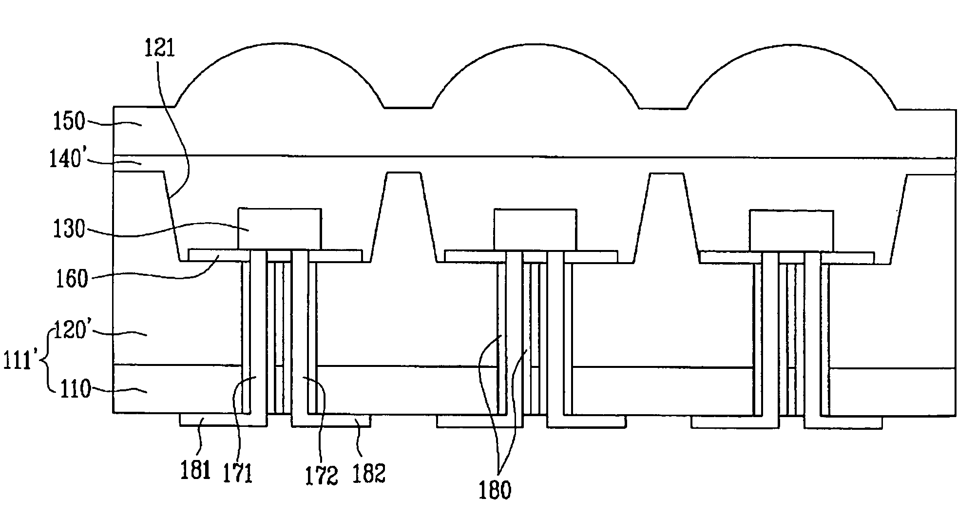
[0029]Exemplary embodiments of the present invention will be described more fully hereinafter with reference to the accompanying drawings, in which exemplary embodiments of the invention are shown. The present invention may, however, be embodied in different forms and should not be construed as being limited to the embodiments set forth herein. Rather, these exemplary embodiments are provided so that this disclosure will be thorough and complete, and will fully convey the scope of the invention to those skilled in the art.

[0030]In the drawings, thickness and / or size of layers, films, and regions are exaggerated for clarity. Like numerals refer to like elements throughout. It will be understood that when an element such as a layer, film, region, or substrate is referred to as being “on” another element, it can be directly on the other element or intervening elements may also be present.

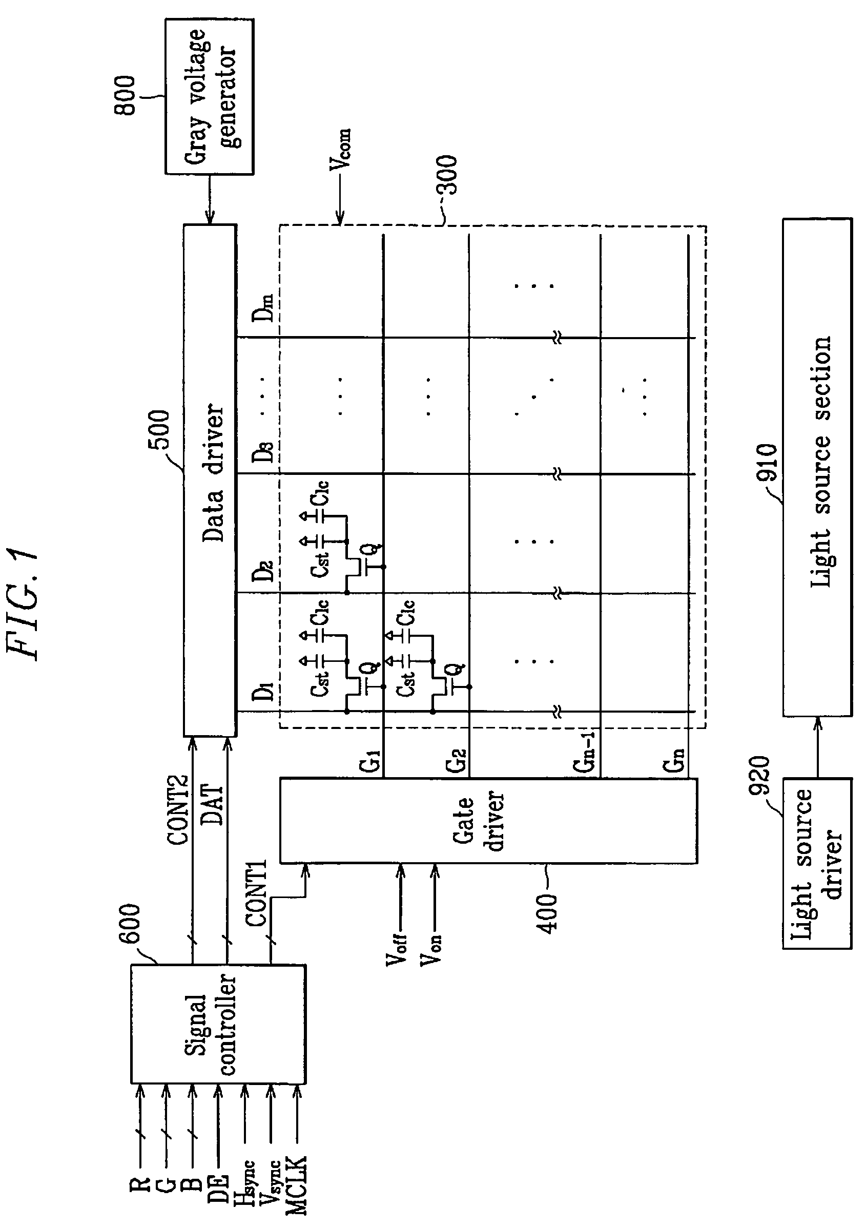
[0031]Hereinafter, a driving system of a light source device for a display device according to exem...


PUM


Abstract

A two-dimensional light source includes a base substrate having holes, wires disposed on a lower surface of the base substrate, a light emitting diode (LED) chip disposed on an upper surface of the base substrate, plugs that connect two electrodes of the LED chip to the wires through the holes, a buffer layer covering the LED chip, and an optical layer that is disposed on the buffer layer and has an optical pattern formed at a portion of the optical layer corresponding to the LED chip.

Description

[0001]This application claims priority to Korean Patent Application No. 2005-007126 filed in the Korean Intellectual Property Office on Jan. 26, 2005, and all the benefits accruing therefrom under 35 U.S.C §119, and the contents of which in its entirety are herein incorporated by reference.BACKGROUND OF THE INVENTION[0002](a) Field of the Invention[0003]The present invention relates generally to a two-dimensional light source using light emitting diodes (LEDs), and more particularly to a surface light source used in backlighting a liquid crystal display (LCD) device and an LCD device using the same.[0004](b) Description of the Related Art[0005]Display devices used to display images, such as television receivers and computer monitors, are classified into self-luminescence display devices capable of self-emitting and light receiving display devices requiring a separate light source. Light emitting diodes (LEDs), electroluminescence (EL) devices, vacuum fluorescent display (VFD) device...

Claims


Application Information

Patent Timeline
Patent Type & Authority Patents(United States)
IPC IPC(8): H01L23/28H01L33/12H01L33/54H01L33/62
CPCG02F1/133603H05K1/0203G02F2001/133607H01L33/58H01L33/62H01L2924/1815H01L2924/19041H05K3/445H05K2201/09481H05K2201/10106H05K2201/10553H01L2224/73265H01L2224/48091H01L2924/00014H01L2224/32225H01L2224/48227H01L2924/00H01L2224/16225H01L2224/49107H01L2224/45139H01L2924/12041H01L2224/05573H01L2224/05568H01L2224/0554G02F1/133607H01L2924/00011H01L2224/05599H01L2224/0555H01L2224/0556H01L2924/00012H01L2224/45015H01L2924/207H01L2924/01049G02F1/1335
Inventor KIM, GI-CHERLPARK, SE-KIYOON, JU-YOUNGYANG, BYUNG-CHOONNAM, SEOK-HYUNLEE, SANG-YU
Owner SAMSUNG DISPLAY CO LTD
Why Eureka
Try Eureka