

Cache memory device, arithmetic processing unit, and its control method
A high-speed cache and control method technology, applied in the direction of electrical digital data processing, calculation, static memory, etc., to achieve the effects of reducing power consumption, avoiding performance degradation, and reducing circuit assembly area
- Summary
- Abstract
- Description
- Claims
- Application Information
AI Technical Summary
Problems solved by technology
Method used
Image

Examples
Embodiment Construction
[0081] An example of an embodiment of the cache line alternation register will be described below with reference to the drawings.
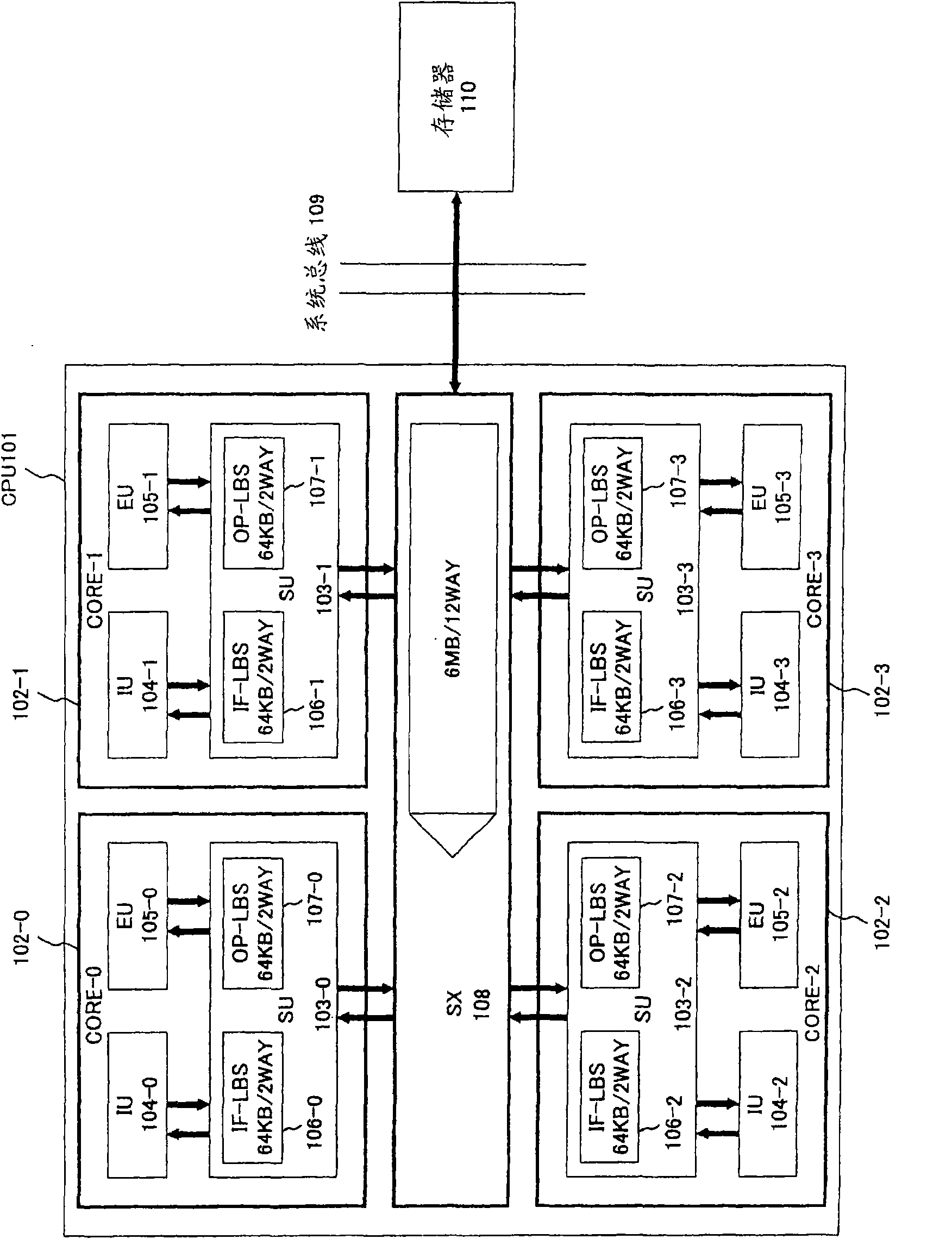
[0082] Figure 8 The overall structure of the CPU of this embodiment is shown.
[0083] Figure 8 The structure of CPU 1 with figure 1 The structure of the CPU 101 shown is substantially the same. CORE2 corresponds to figure 1 CORE 102, SU 3 corresponds to figure 1 SU 103, IU4 corresponds to figure 1 IU 104, EU 5 corresponds to figure 1 EU 105, IF-LBS 6 corresponds to figure 1 IF-LBS 106, OP-LBS 7 correspond to figure 1 The OP-LBS 107, SX 10 corresponds to figure 1 SX 108, SYSTEM BUS 11, Memory 12 respectively correspond to figure 1 SYSTEM BUS 109, Memory 110.
[0084] In this embodiment, IF-CLAR (Cache Line Alternation Register: cache line alternation register) 8 and OP-CLAR 9 are newly added.
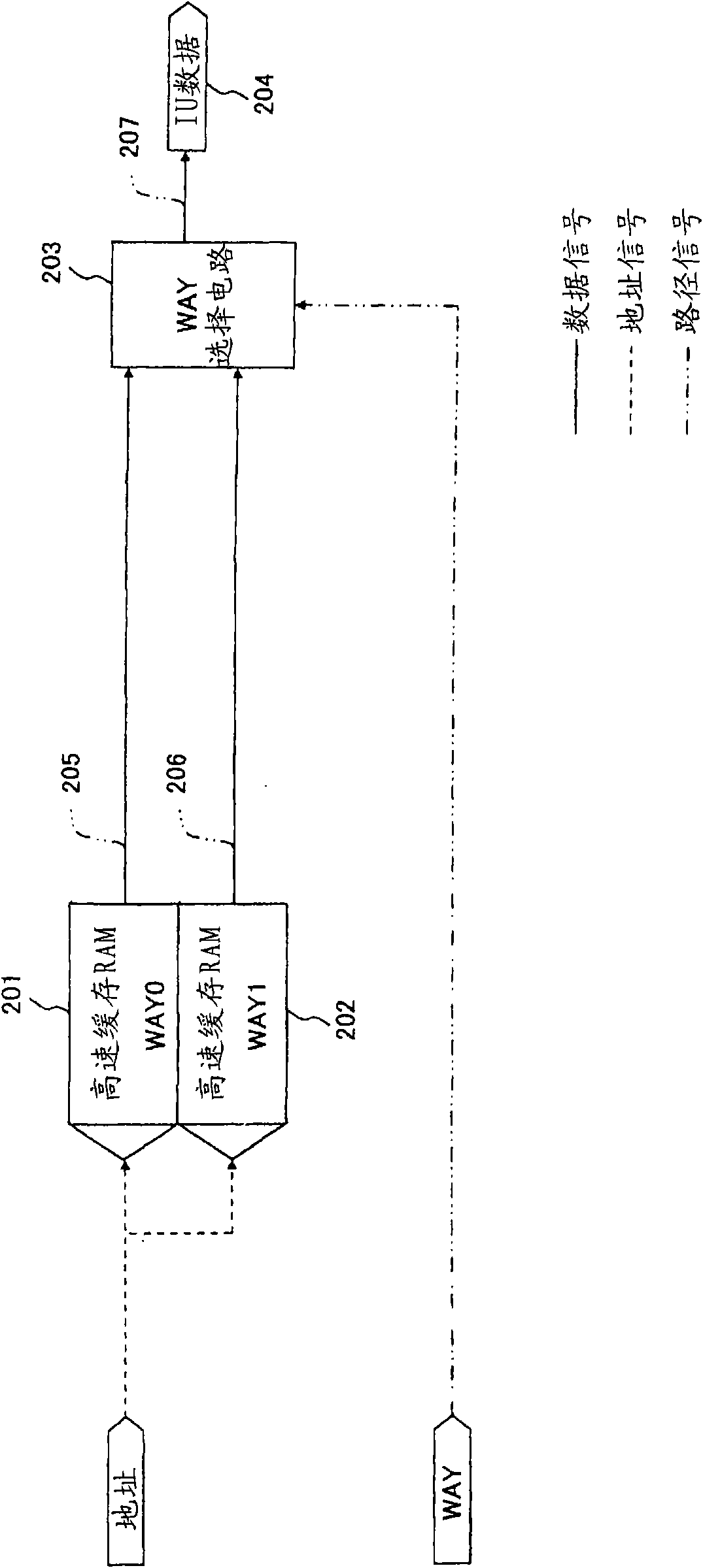
[0085] Figure 9 The structure of the cache line alternation register CLAR of this embodiment is shown, and figure 2 A comparison reveals ...
PUM
 Abstract
Description
Claims
Application Information