
Flash chip detecting method based on boundary scan

A technology of chip detection and boundary scan, applied in the direction of measuring electricity, measuring devices, measuring electrical variables, etc., can solve the problems of lack of systematic testing and limitations of chip testing versatility

Inactive Publication Date: 2010-05-26
NANJING UNIV OF AERONAUTICS & ASTRONAUTICS
View PDF0 Cites 5 Cited by
  • Summary
  • Abstract
  • Description
  • Claims
  • Application Information

AI Technical Summary

Problems solved by technology

[0005] For the Flash chip that does not support the JTAG standard boundary scan, it does not yet have the function of systematic testing, so it is greatly limited in the universality of chip testing

Method used


Image

  • Flash chip detecting method based on boundary scan
  • Flash chip detecting method based on boundary scan
  • Flash chip detecting method based on boundary scan

Examples

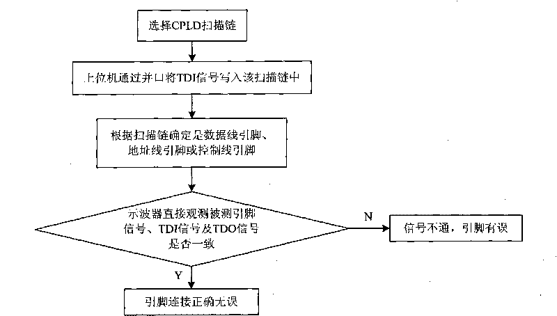

Embodiment Construction

[0023] The working principle of the present invention is as follows:

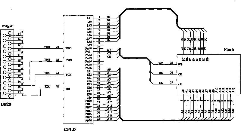
[0024] Connect the JTAG test ports TDI, TMS, TCK, and TDO of the CPLD chip to the parallel port of the upper PC, and write the control instructions and target codes to the JTAG port from the parallel port of the PC to the BSR (Boundary Scan Register) of JTAG through the program , BSR is composed of BSC (Boundary Scan Cell) connected in series. When designing the PCB, connect the data scan chain, address scan chain, and control scan chain of the CPLD to the data lines, address lines, and control lines of the Flash chip under test. There are corresponding signals sent to its BSC on the pins of the BSC, and the signals can be sent to the Flash under test through the corresponding pins of the BSC.

[0025] Among the present invention, CPLD chip adopts the CPLD device LFXP2_5E_XXQ208 of Lattic Company, combines figure 1 with image 3 Shown, method flow process of the present invention is as follows:

[0026]...


PUM


Abstract

The invention discloses a flash chip detecting method based on boundary scan, belonging to the field of boundary scan of chips. The method comprises the steps of: firstly, respectively connecting pins of three kinds of signal lines comprising data lines, address lines and control lines of the Flash chip to be detected with pins of any one of scan chains of a CPLD chip; then connecting the parallel port of a principal personal computer (PC) with four JTAG pins of the CPLD chip; sending binary signals to the corresponding pins to be detected from the principal PC through TDI pins; and observing the waveforms of the corresponding signals through an oscillograph to judge the correctness of the connection of the pins. In the invention, the JTAG detection of the CPLD chip is used for indirectly detecting the Flash chip without JTAG interfaces; and the method of the invention has convenient operation, low hardware cost and low testing cost, can be used for testing multiple control circuits, and reduces the quantity of peripheral testing interfaces.

Description

technical field [0001] The invention relates to a chip detection method, in particular to a boundary scan-based Flash chip detection method, which belongs to the field of chip boundary scan. Background technique [0002] SoC (System On a Chip) design is becoming increasingly complex, which not only increases the chip area, but also sharply reduces the testability of circuits and systems. The proportion of time consumed in SoC design is increasing. Conventional testing methods are facing increasing testing difficulties. [0003] With the shortening of the design and test cycle, it has become an inevitable trend to combine test and design to complete DFT (Design for Test-ability). As an important design-for-test technology, boundary-scan technology can not only test the debug function of the entire SoC or PCB, but also test whether there is any fault in the connection between modules. In 1990, IEEE and JTAG (Joint Test Action Group) jointly formulated the JTAG boundary scan ...

Claims


Application Information

Patent Timeline
IPC IPC(8): G01R31/3185
Inventor 高尚丰立东顾娜陈亮亮安逸
Owner NANJING UNIV OF AERONAUTICS & ASTRONAUTICS
Learn More