
Electronic device structure

An electronic device, combined with column technology, applied in the direction of electrical digital data processing, digital processing power distribution, instruments, etc., can solve the problems of loosening, poor fixing effect, damage to the ball grid array packaging structure, etc., to achieve good buffer capacity, avoid Deformation or destruction effects

Inactive Publication Date: 2010-05-26
湖南格致测控技术有限公司
View PDF0 Cites 3 Cited by
  • Summary
  • Abstract
  • Description
  • Claims
  • Application Information

AI Technical Summary

Problems solved by technology

Although Patent No. 576515 provides a good cushioning capacity for the motherboard, the pins are prone to loosening due to the aging of the material after long-term use, and the fixing effect is not as good as that of screw locking.
[0006] Especially for Ball Grid Array (BGA) motherboards, no matter whether the motherboard is fixed with screws or fixed with pins, when the screws are locked or the pins are inserted into the pins In the hole, the main board will not be able to produce horizontal displacement (that is, the direction of the X-axis and the Y-axis) due to the holding of the screw or the bolt, so the stress on the main board will only be generated in the vertical direction (that is, the direction of the Z-axis) Deformation, which will cause the ball grid array package structure of the motherboard to be damaged, resulting in the loss of electrical connection between the chip and the motherboard

Method used


Image

  • Electronic device structure
  • Electronic device structure
  • Electronic device structure

Examples


Embodiment Construction

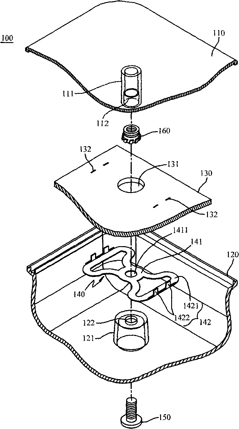
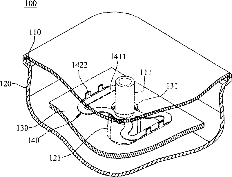
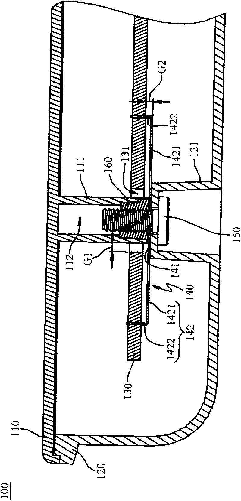
[0043] According to the structure of the electronic device disclosed in the present invention, the electronic device includes but is not limited to portable computer devices such as notebook computers, tablet computers, ultra-mobile computers (UMPCs), and personal digital assistants (PDAs). limit. In the following detailed description of the present invention, a notebook computer will be taken as the preferred embodiment of the present invention. However, the accompanying drawings are provided for reference and illustration only, and are not intended to limit the present invention.

[0044] see Figure 1 to Figure 3 The electronic device 100 according to the first embodiment of the present invention includes an upper case 110 , a lower case 120 , a main board 130 , a suspension 140 , and a fixing part 150 . The inner side of the upper casing 110 is protrudingly provided with an upper coupling column 111, and the upper coupling column 111 has a fixing hole 112, wherein a nut ...


PUM


Abstract

The invention relates to an electronic device structure which comprises an upper casing body, a lower casing body, a mainboard, a suspending element and a fixing element, wherein the upper casing body and the lower casing body are separately provided with an upper binding post and a lower binding post correspondingly. The mainboard is arranged between the upper casing body and the lower casing body, and is provided with a through hole. The upper binding post penetrates through the through hole, the size of the through hole is greater than that of the upper binding post, and then a gap is formed between the upper binding post and the through hole. The suspending element is arranged between the mainboard and the lower casing body, and is combined with one side of the mainboard, and a suspending space is formed between the suspending element and the mainboard. The fixing element penetrates through the lower binding post and the suspending element, and is fixed on the upper binding post, and then the mainboard is arranged on the lower binding post by the suspending element. In the invention, the movable space and the suspending space generated by the size matching of the through hole and the upper binding post and the arrangement of the suspending element are utilized to ensure that the mainboard has displacement in three axis directions, thereby good buffer capability is provided, and the deformation or damage of the mainboard caused by external force impact or stress is avoided.

Description

technical field [0001] The present invention relates to an electronic device, in particular to an electronic device structure in which a motherboard can be displaced in three-axis directions. Background technique [0002] Nowadays, with the rapid development of science and technology, computer equipment has become an indispensable product in work or life, and the development trend of electronic products is gradually developing towards miniaturized, thin, light and short products. For users who often need to move outside, Portable electronic products such as notebook computers (Notebook) have become easier to carry, greatly improving the convenience of use. A motherboard must be installed inside the notebook computer as a core component of the computer system, and can smoothly execute preset functions of peripheral hardware electrically connected to the motherboard. [0003] The current common way to fix the mainboard is to arrange a plurality of conductive copper pillars (b...

Claims


Application Information

Patent Timeline
IPC IPC(8): G06F1/16G06F1/18
Inventor 廖飞钦
Owner 湖南格致测控技术有限公司
Learn More