Method for writing in and reading out data based on virtual block flash memory address mapping

A technology of address mapping and data writing, applied in the direction of memory address/allocation/relocation, input/output to the record carrier, etc., can solve the problems of increasing speed, not taking advantage of channel parallelism, etc., to prolong life and improve utilization. , Improve the effect of reading and writing speed

Inactive Publication Date: 2010-06-09
XIAN KEYWAY TECH
View PDF0 Cites 33 Cited by
  • Summary
  • Abstract
  • Description
  • Claims
  • Application Information

AI Technical Summary

Problems solved by technology

[0005] The purpose of the present invention is to provide a data writing and reading method based on virtual block flash memory address mapping, which solves the technical problem of not using the parallel advantages in the channel to improve the speed in the background technology

Method used


Image

  • Method for writing in and reading out data based on virtual block flash memory address mapping
  • Method for writing in and reading out data based on virtual block flash memory address mapping
  • Method for writing in and reading out data based on virtual block flash memory address mapping

Examples


Embodiment Construction

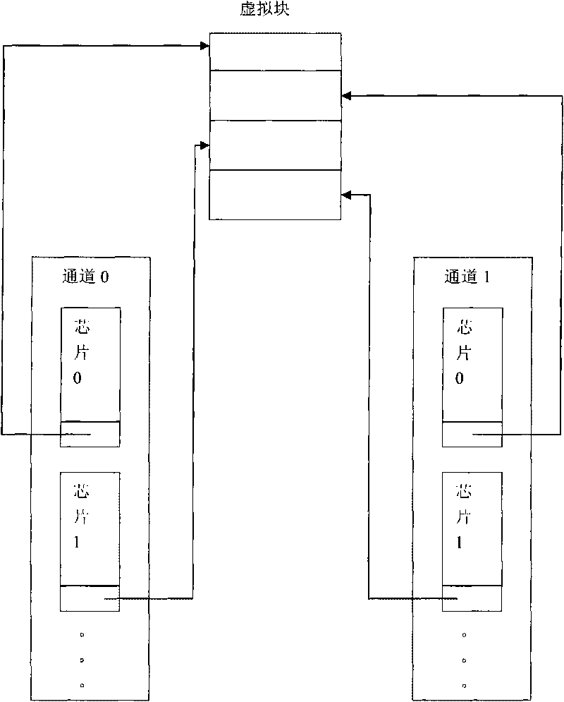
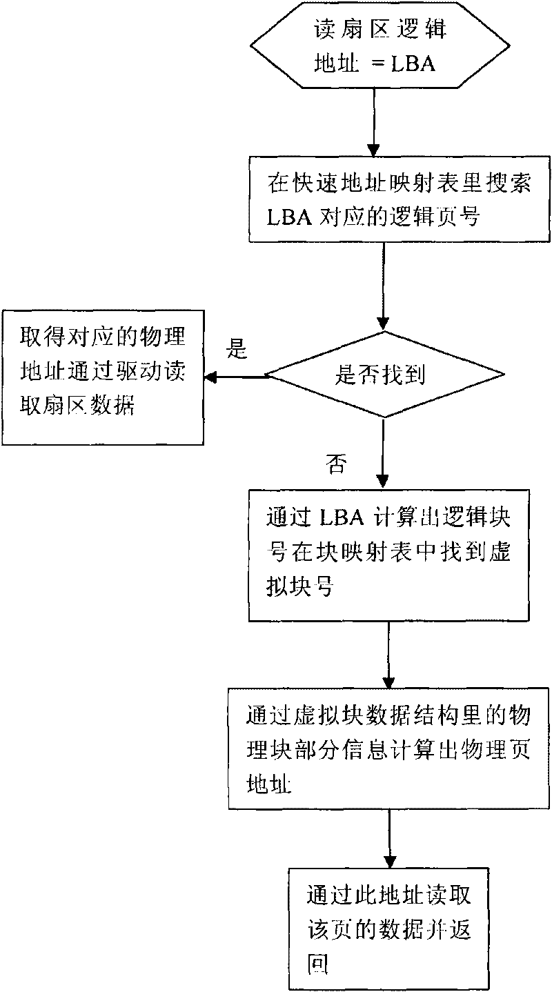
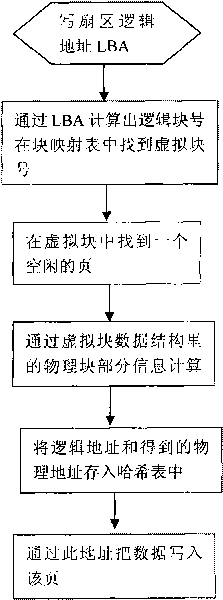
[0038] see figure 1 , figure 2 and image 3 , a data writing and reading method based on virtual block flash memory address mapping, the method comprises the following steps:

[0039] 1) Build a virtual block

[0040] The composition of the virtual block is composed of a part of the physical block in each chip in each channel. Specifically, each physical block is divided into N blocks, and then a 1 / n physical block is taken in each chip in each channel. Blocks to form a virtual block; each virtual block is composed of a data structure, which records the part of the virtual block composed of those physical blocks;

[0041] 2) Build an initial address mapping table

[0042] The initial address mapping table includes a logical address page number and a physical address page number;

[0043] The logical address page number is a logical address given by the upper computer, and the index of the virtual block number is obtained by moduloing the number of sectors contained in th...


PUM


Abstract

The invention relates to a method for writing in and reading out data based on virtual block flash memory address mapping. The method is characterized by comprising the following steps of: building a virtual block, building an initial address mapping table, writing in data and reading out the data. The method solves the technical problem on increasing the speed without utilizing the parallel advantages in a passage, has the advantage of mapping the data in a plurality of chips in a plurality of passages so as to simultaneously carry out the parallel operations of the passages and the parallel operations in the passages for increasing the read-write speed under the circumstance of continuous logic addresses of user data. Meanwhile, the invention can be used for building a virtual block under the circumstance of idleness of a physical block, thereby increasing the utilization rate of the physical block and prolonging the service life of the flash memory chip.

Description

technical field [0001] The invention relates to a data writing and reading method of a flash memory controller, in particular to a data writing and reading method of a flash memory controller based on virtual block flash memory address mapping. Background technique [0002] SSD is the abbreviation of solid state disk in English, that is, solid state disk, which is a kind of memory that uses Nand flash chip as a storage medium. It has the advantages of fast data access speed, durability, shockproof and drop resistance, very quiet work without any noise, etc. [0003] The core component of the solid-state disk is the flash memory controller, whose function is to control and manage the flash memory chip and provide a standard interface to the outside. In order to increase the speed of the solid state disk, the flash memory controller controls multiple flash memory chips at the same time, that is, multiple channels. Each channel can have multiple chips, and each channel can wor...

Claims


Application Information

Patent Timeline
Patent Type & Authority Applications(China)
IPC IPC(8): G06F3/06G06F12/06
Inventor 邱波
Owner XIAN KEYWAY TECH
Why Eureka
Try Eureka