
Solid-state imaging device, manufacturing method of the same, and imaging apparatus

By forming a thin film gate electrode on a semiconductor substrate, the problem of difficulty in installing planar CMOSFETs and vertical transistors at the same time in the existing technology is solved, higher refinement and density packaging are achieved, and image processing speed and accuracy are improved.

Inactive Publication Date: 2010-06-09
SONY GRP CORP
View PDF13 Cites 5 Cited by
  • Summary
  • Abstract
  • Description
  • Claims
  • Application Information

AI Technical Summary

Problems solved by technology

[0009] It is necessary to solve the problem of difficulty in mounting both planar CMOSFETs and vertical transistors on the same semiconductor substrate

Method used


Image

  • Solid-state imaging device, manufacturing method of the same, and imaging apparatus
  • Solid-state imaging device, manufacturing method of the same, and imaging apparatus
  • Solid-state imaging device, manufacturing method of the same, and imaging apparatus

Examples


no. 1 example

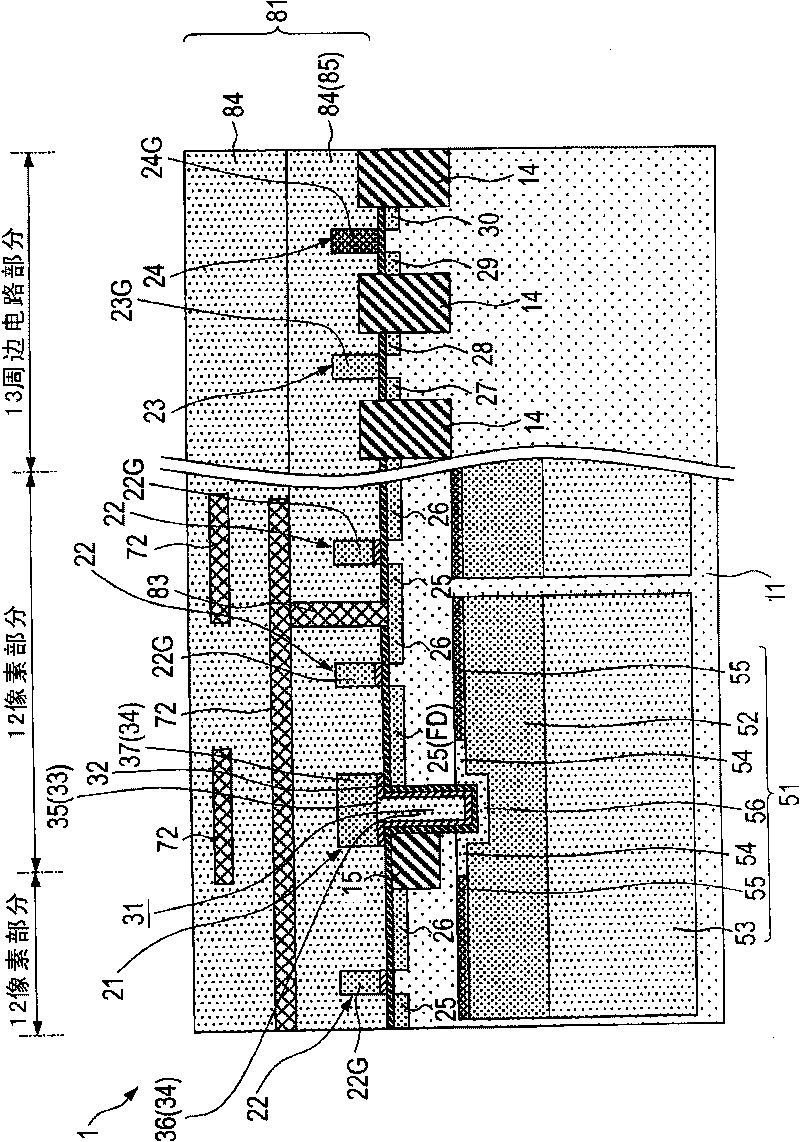
[0102] [First Example of Configuration of Solid-State Imaging Device]

[0103] will use figure 1 A schematic configuration sectional view of FIG. 1 illustrates an example (first example) of the configuration of the solid-state imaging device according to the first embodiment of the present invention.

[0104] Such as figure 1 As shown, in the semiconductor substrate 11, a photoelectric conversion portion 51 that photoelectrically converts incident light to obtain an electric signal is formed. Further, in the semiconductor substrate 11 , the pixel portion 12 is formed including a vertical transistor 21 that reads signal charges from the photoelectric conversion portion 51 and a planar transistor 22 that processes the read signal charges. In addition, a peripheral circuit portion 13 is formed on the periphery of the pixel portion 12 . The peripheral circuit section 13 has a first conductivity type (hereinafter, eg N type) channel transistor (hereinafter referred to as NFET) 2...

no. 3 example

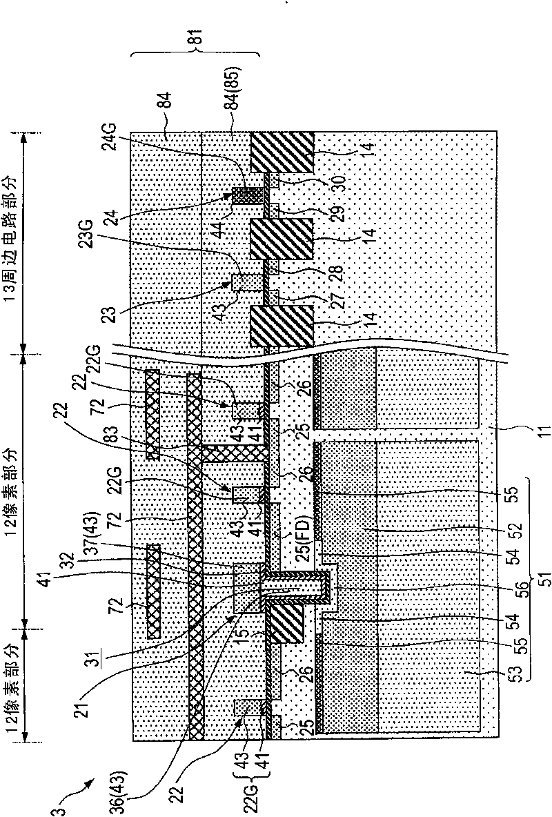
[0174] [Third Example of Configuration of Solid-State Imaging Device]

[0175] will use image 3 The schematic configuration cross-sectional view of is an illustration of an example of the configuration of a solid-state imaging device according to a third embodiment of the present invention (third example).

[0176] Such as image 3 As shown, in the semiconductor substrate 11, a photoelectric conversion portion 51 that photoelectrically converts incident light to obtain an electrical signal is formed. Further, in the semiconductor substrate 11 , the pixel portion 12 is formed including a vertical transistor 21 that reads signal charges from the photoelectric conversion portion 51 and a planar transistor that processes the read signal charges. In addition, a peripheral circuit portion 13 is formed on the periphery of the pixel portion 12 . The pixel circuit section 13 has a first conductivity type (hereinafter, eg N type) channel transistor (hereinafter referred to as NFET) ...

no. 4 example

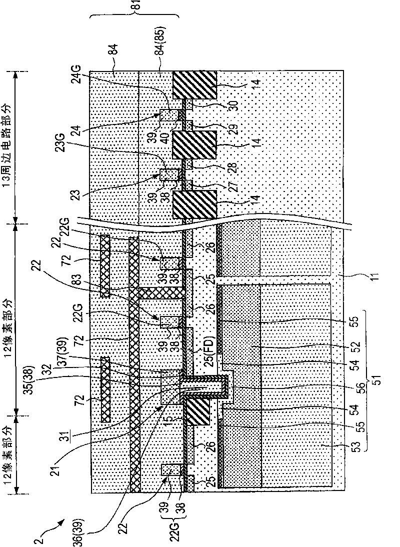
[0216] [Fourth Example of Configuration of Solid-State Imaging Device]

[0217] will use Figure 4 The schematic configuration cross-sectional view of is an illustration of an example of the configuration of a solid-state imaging device according to a fourth embodiment of the present invention (fourth example).

[0218] Such as Figure 4 As shown, in the semiconductor substrate 11, a photoelectric conversion portion 51 that photoelectrically converts incident light to obtain an electrical signal is formed. Further, in the semiconductor substrate 11 , the pixel portion 12 is formed including a vertical transistor 21 that reads signal charges from the photoelectric conversion portion 51 and a planar transistor that processes the read signal charges. In addition, a peripheral circuit portion 13 is formed on the periphery of the pixel portion 12 . The pixel circuit section 13 has a first conductivity type (hereinafter, eg N type) channel transistor (hereinafter referred to as N...


PUM


Abstract

The invention discloses a solid-state imaging device, a manufacturing method of the same and an imaging apparatus. The solid-state imaging device on a semiconductor substrate includes: a pixel part having a photoelectric conversion part photoelectrically converting incident light to obtain signal charge; and a peripheral circuit part formed on a periphery of the pixel part on a semiconductor substrate. The pixel part having a vertical transistor that reads out the signal charge from the photoelectric conversion part and a planar transistor that processes the signal charge read out by the vertical transistor. The vertical transistor has a groove part formed on the semiconductor substrate; a gate insulator film formed on an inner surface of the groove part; a conducting layer formed on a surface of the gate insulator film on the semiconductor substrate within and around the groove part; a filling layer filling an interior of the groove part via the gate insulator film and the conducting layer; and an electrode layer connected to the conducting layer on the filling layer.

Description

technical field [0001] The present invention relates to a solid-state imaging device, a manufacturing method thereof, and an imaging apparatus. Background technique [0002] A solid-state imaging device including both vertical transistors and planar transistors is disclosed (for example, see JP-A-2005-223084). [0003] It is difficult to fabricate vertical transistors and CMOSFETs including planar transistors (eg, CMOSFETs following design rules below 0.18um) on the same substrate. [0004] For example, a case where non-doped polysilicon is used for each gate electrode of a vertical transistor and a planar transistor will be described. [0005] When the vertical hole of the vertical transistor is filled with non-doped polysilicon for the gate electrode and closed, it is difficult to dope the polysilicon in a deeper portion of the vertical hole of the substrate. [0006] For example, there is a method that fills vertical holes forming vertical transistors with polysilicon, ...

Claims


Application Information

Patent Timeline
Patent Type & Authority Applications(China)
IPC IPC(8): H01L27/146H01L21/82H04N5/335H01L21/8234H01L21/8238H01L27/088H01L27/092
CPCH01L27/14614H01L27/14689H01L27/14634H01L29/66666
Inventor 太田和伸平野智之
Owner SONY GRP CORP
Learn More