Silicon wafer bearing table for photoetching machine and use method thereof

A technology of a bearing table and a lithography machine, which is used in microlithography exposure equipment, photolithography process exposure devices, etc., can solve problems such as affecting the quality of products in subsequent operations, waste of lithography resources, affecting product quality, etc., and avoid frontal graphics. Out-of-focus phenomenon, reduce manufacturing cost, reduce the effect of lithography rework

Active Publication Date: 2010-06-16
SHANGHAI HUAHONG GRACE SEMICON MFG CORP
View PDF0 Cites 7 Cited by
  • Summary
  • Abstract
  • Description
  • Claims
  • Application Information

AI Technical Summary

Problems solved by technology

Seriously affected silicon wafers and even lithography rework cannot solve the problem and affect product quality
[0003] If the particles on the silicon wafer fall on the carrier platform, it will also affect the product quality of subsequent operations, resulting in a waste of lithography resources and an increase in production costs.

Method used


Image

  • Silicon wafer bearing table for photoetching machine and use method thereof
  • Silicon wafer bearing table for photoetching machine and use method thereof
  • Silicon wafer bearing table for photoetching machine and use method thereof

Examples


Embodiment Construction

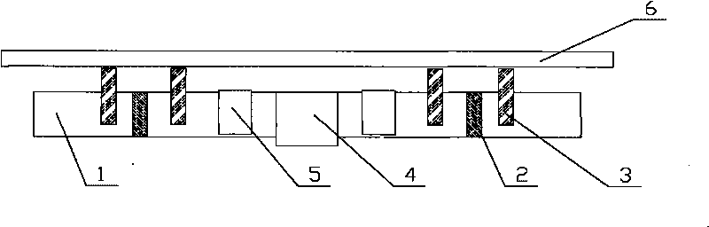
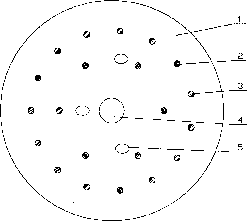
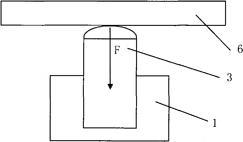
[0024] Such as figure 1 , figure 2 As shown, the silicon wafer carrying platform of the lithography machine of the present invention includes a carrying platform base 1, a vacuum hole 2, a stress sensor 3, a connector 4, and a silicon wafer receiving device 5; the carrying platform base 1 is provided with a plurality of vacuum The hole 2 and the silicon chip receiver 5; the bottom of the carrier base 1 is provided with a connector 4.

[0025] The vacuum hole 2 is used for vacuuming the silicon wafer 6 to fix the silicon wafer 6 . The silicon wafer receiver 5 is used for receiving and sending the silicon wafer 6 . There is a clearance fit between the carrier base 1 and the silicon wafer transfer device 5 , and the silicon wafer transfer device 5 can stretch up and down on the carrier base 1 to facilitate the transfer of the silicon wafer 6 . The connector 4 fixes the stage base 1 on the photolithography machine.

[0026] The shape of the carrier base 1 can be circular, rec...


PUM


Abstract

The invention discloses a silicon wafer bearing table for a photoetching machine, which comprises a bearing table base, a plurality of vacuum holes, a plurality of stress inductors, a connector and a silicon wafer transfer device, wherein the plurality of vacuum holes and the silicon wafer transfer device are arranged on the bearing table base; the connector is arranged at the bottom of the bearing table base; and the stress inductors are arranged on the surface of the bearing table base. The stress inductors are connected with an electric power conversion circuit of which the output end is connected with a terminal controller, and the terminal controller is connected with a power motor. The stress inductors realize expansion and regulate height by inducting the information of action points, magnitudes, directions and the like of acting force from silicon wafers. By regulating the height of each stress inductor which is in contact with the silicon wafers, the silicon wafer bearing table for the photoetching machine of the invention can ensure that the front sides of the silicon wafers are on the same horizontal plane at all times, thereby preventing the images on the front sides from being out of focus caused by contaminants of particles and the like on the back sides of the silicon wafers, and reducing rework of photoetching. The invention also discloses a use method of the silicon wafer bearing table for the photoetching machine.

Description

technical field [0001] The invention relates to semiconductor manufacturing equipment, in particular to a photolithography machine silicon wafer carrier, and the invention also relates to a method for using the photolithography silicon wafer carrier. Background technique [0002] In the currently used silicon wafer carrier, the surface in contact with the silicon wafer is fixed. Using this silicon chip carrier, if the back side of the silicon chip has dirt such as particles, the front side of the silicon chip is not on the same level. When the photolithography machine is exposed, the front pattern area corresponding to the particles on the silicon wafer will be defocused, resulting in a change in the shape of the photolithographic pattern, and the affected silicon wafer needs to be photolithographically reworked. Seriously affected silicon wafers and even lithography rework cannot solve the problem and affect product quality. [0003] If the particles on the silicon wafer ...

Claims


Application Information

Patent Timeline
Patent Type & Authority Applications(China)
IPC IPC(8): G03F7/20
Inventor 宁开明
Owner SHANGHAI HUAHONG GRACE SEMICON MFG CORP
Why Eureka
Try Eureka