Manufacturing method of shallow trench structure

A fabrication method and shallow trench technology, applied in semiconductor/solid-state device manufacturing, electrical components, circuits, etc., can solve problems such as damage to silicon substrates, degradation of semiconductor device quality, thinning of film thickness, etc., to improve the stress environment , improve the electrical performance, avoid the effect of damage

Inactive Publication Date: 2010-06-16
SEMICON MFG INT (SHANGHAI) CORP
View PDF0 Cites 11 Cited by
  • Summary
  • Abstract
  • Description
  • Claims
  • Application Information

AI Technical Summary

Problems solved by technology

In the process of forming the filled oxide layer, the plasma will continuously bombard the substrate oxide layer, especially for the sharp part of the substrate oxide layer located at each corner of the shallow trench, the plasma erosion will be more obvious, and the film The thickness of the l

Method used


Image

  • Manufacturing method of shallow trench structure
  • Manufacturing method of shallow trench structure
  • Manufacturing method of shallow trench structure

Examples


Example Embodiment

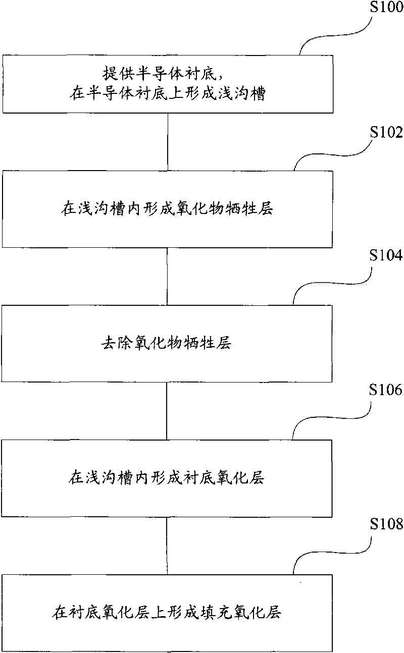
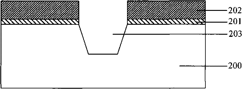
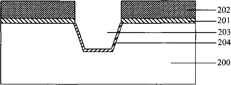
[0019] The inventors found that when making the shallow trench structure, the corners of the shallow trench are sharp, and when the filling oxide layer is formed by the HDP-CVD process, because HDP has a certain etching ability, the plasma oxidizes the substrate. The substrate oxide layer is bombarded, and the thickness of the substrate oxide layer is small, especially the substrate oxide layer at each corner of the shallow trench is also sharp, so the substrate oxide layer is very easy to be destroyed under plasma bombardment, resulting in filling oxidation. The layer is directly in contact with the silicon substrate in the shallow trench, so that the stress in the shallow trench changes, and even destroys the lattice in the shallow trench, causing defects in the lattice, resulting in a decrease in the electrical performance of the semiconductor device.

[0020] Therefore, in the manufacture of semiconductor devices, in order to prevent the above-mentioned defects from affecti...


PUM

PropertyMeasurementUnit
Thicknessaaaaaaaaaa

Abstract

The invention relates to a manufacturing method of a shallow trench structure, which comprises the following steps of: providing a semiconductor substrate and forming a shallow trench on the semiconductor substrate; forming an oxide sacrifice layer in the shallow trench; removing the oxide sacrifice layer; forming a substrate oxide layer in the shallow trench; and forming a filling oxide layer for filling the shallow trench on the substrate oxide layer. Through the technical scheme, a corner at the top end of the shallow trench can be rounded in the forming process, thereby improving the stress environment in the shallow trench, avoiding the damage of a subsequent process to the shallow trench, improving the electrical performance of a semiconductor device and enhancing the yield of a semiconductor product.

Description

technical field [0001] The invention relates to the technical field of semiconductor manufacturing, in particular to a method for manufacturing a shallow trench structure. Background technique [0002] The development direction of semiconductor integrated circuits is to increase density and shrink components. In the manufacture of integrated circuits, the isolation structure is an important technology, and the components formed on the silicon substrate must be isolated from other components. With the advancement of semiconductor manufacturing technology, shallow trench isolation (Shallow Trench Isolation, STI) technology has gradually replaced other isolation methods such as local oxidation of silicon (LOCOS) used in traditional semiconductor device manufacturing. [0003] The manufacturing method of the existing shallow trench isolation structure generally includes: oxidizing the silicon wafer in a high-temperature oxidation furnace tube, forming a pad oxide layer (Pad Oxi...

Claims


Application Information

Patent Timeline
IPC IPC(8): H01L21/762
Inventor 韩秋华杜珊珊黄怡赵林林
Owner SEMICON MFG INT (SHANGHAI) CORP
Why Eureka
Try Eureka