Pin and substrate combined semiconductor package and manufacturing method thereof
A semiconductor and packaging technology, applied in the field of semiconductor packaging, can solve the problems of limited increase in the number of input/output connections, complex and messy circuit layout, and inability to flexibly adjust the position, so as to achieve the effect of improving transmission efficiency
- Summary
- Abstract
- Description
- Claims
- Application Information
AI Technical Summary
Problems solved by technology
Method used
Image
Examples
no. 1 example
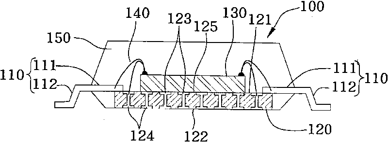
[0049] see figure 1 , is a schematic cross-sectional view of a first embodiment of a semiconductor package combined with leads and a substrate of the present invention. As shown in the figure, the semiconductor package 100 combined with leads and a substrate of this embodiment includes: a plurality of leads 110 , a substrate 120 , a semiconductor chip 130 , a plurality of bonding wires 140 and an encapsulant 150 . Each of the pins 110 has an inner pin 111 and an outer pin 112; Placement area 125 and a plurality of pads 123, a plurality of electrical connection pads 124 are formed on the second surface 122, and each lead 110 is connected to the first surface 121 of the substrate 120 with its inner lead 111 so that after each guide pin 110 is combined with the substrate 120, the outer guide pin 112 of each guide pin 110 protrudes outward from the edge of the substrate 120; the semiconductor chip 130 is connected to the first surface 121 of the substrate 120 Chip landing area ...
no. 2 example
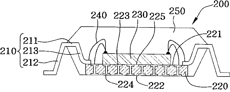
[0052] see figure 2 , is a schematic cross-sectional view of the second embodiment of the semiconductor package combined with the lead and the substrate of the present invention. As shown in the figure, the semiconductor package 200 combined with the lead and the substrate of the present invention and the previous embodiment include: A lead 210 , a substrate 220 , a semiconductor chip 230 , a plurality of bonding wires 240 and an encapsulant 250 . Different from the previous embodiment, the inner guide pin 211 of each guide pin 210 is further bent upward to form a bent portion 213 to increase the height of the outer guide pin 212 so that a bottom of the guide pin 210 is formed. space, and can be used as circuit layout of other electronic components; and the substrate 220 has a first surface 221 and a second surface 222 opposite to the first surface 221 as in the previous embodiment, and on the first surface 221 There is a chip landing area 225 and a plurality of welding pads...
no. 3 example
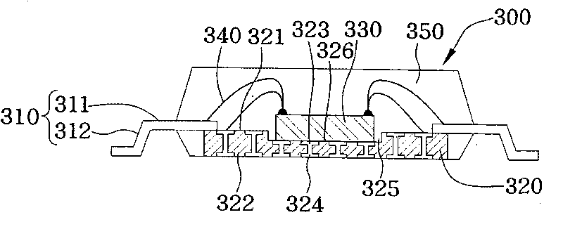
[0055] see image 3 , is a schematic cross-sectional view of the third embodiment of the semiconductor package combined with the lead and the substrate of the present invention, as shown in the figure, the semiconductor package 300 combined with the lead and the substrate of the present invention includes the same as the first two embodiments : a plurality of leads 310 , a substrate 320 , a semiconductor chip 330 , a plurality of bonding wires 340 and an encapsulation compound 350 . Each of the pins 310 has an inner pin 311 and an outer pin 312; Placement area 326 and a plurality of pads 323, a plurality of electrical connection pads 324 are formed on the second surface 322, and each lead 310 is connected to the first surface 321 of the substrate 320 with its inner lead 311 so that after each guide pin 310 is combined with the substrate 320, the outer guide pin 312 of each guide pin 310 protrudes outward from the edge of the substrate 320; the semiconductor chip 330 is connec...
PUM
 Abstract
Description
Claims
Application Information


