Silicon slice optimal scheduling method and device

A technology for optimizing scheduling and silicon wafers, which is applied in the direction of comprehensive factory control, comprehensive factory control, electrical program control, etc., can solve problems such as unsatisfactory processing equipment, and achieve the effects of increasing productivity, improving execution efficiency, and increasing concurrency

Active Publication Date: 2010-06-23
BEIJING NAURA MICROELECTRONICS EQUIP CO LTD
View PDF0 Cites 10 Cited by
  • Summary
  • Abstract
  • Description
  • Claims
  • Application Information

AI Technical Summary

Problems solved by technology

[0012] However, under normal circumstances, the smallest unit of the transmission sequence calculated by Scheduler is the internal module of the device, that is, only the source

Method used


Image

  • Silicon slice optimal scheduling method and device
  • Silicon slice optimal scheduling method and device
  • Silicon slice optimal scheduling method and device

Examples


Embodiment 1

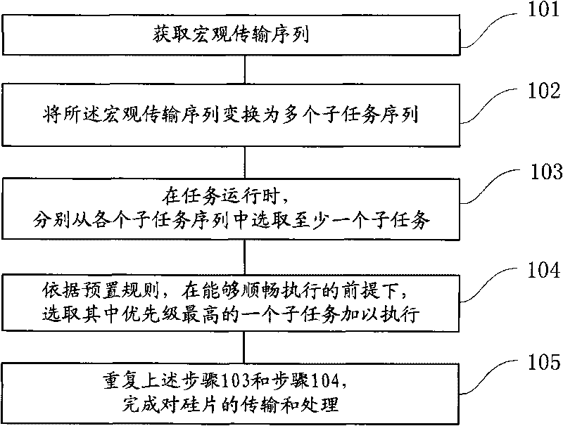
[0069] refer to figure 1 , which shows an embodiment 1 of a method for optimal scheduling of silicon wafers according to the present invention, which may specifically include the following steps:

[0070] Step 101, obtaining a macro transmission sequence (macro transmission sequence);

[0071] Step 102, converting the macro transmission sequence into multiple subtask sequences (or called multiple subtask sequences);

[0072] As specific to the device, the simplest transfer action is also completed by the transfer-related modules, so the execution actions in the macro transfer sequence can be further subdivided. For example, a transfer action can be divided into two subtasks: fetching and putting.

[0073] In the present invention, the macro transmission sequence calculated by the Scheduler module is further subdivided into smaller subtask sequences according to the execution actions of each module, and this series of subtask sequences is finally executed. In the present inv...

Embodiment 2

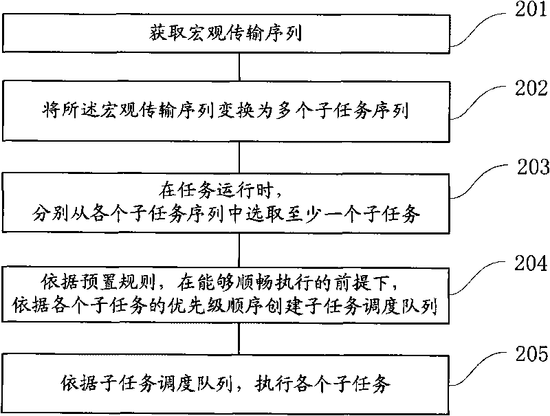
[0146] refer to figure 2 , shows Embodiment 2 of a method for optimal scheduling of silicon wafers according to the present invention, which may specifically include the following steps:

[0147] Step 201, obtaining a macro transmission sequence;

[0148] Step 202, converting the macro transmission sequence into a plurality of subtask sequences;

[0149] Step 203, when the task is running, select at least one subtask from each subtask sequence;

[0150]Step 204, according to preset rules, on the premise of smooth execution, create a subtask scheduling queue according to the priority order of each subtask;

[0151] Step 205: Execute each subtask according to the subtask scheduling queue.

[0152] This example and figure 1 The illustrated embodiments are basically similar, so the similarities will not be repeated. What needs to be emphasized in Embodiment 2 is that it is not like Embodiment 1, which performs a sorting judgment after each subtask is executed, and then execut...


PUM


Abstract

The invention discloses a silicon slice optimal scheduling method, which comprises the following steps: a, acquiring a macro transmission sequence; b, converting the macro transmission sequence into a plurality of sub task sequences; c, when a task is run, selecting at least one sub task from each sub task subsequence; d, according to preset rules, on the premise of smooth execution, executing a sub task with the highest priority; and e, repeating the steps c and d and completing the transmission and processing of silicon slices. In the invention, on the basis of the macro transmission sequence, a lower layer micro transmission sequence execution policy is optimized, so the concurrency of the execution of the sub tasks is improved, the execution efficiency of Job is improved and consequently yield of a machine is increased.

Description

technical field [0001] The invention relates to the technical field of process data processing, in particular to a method and device for optimal scheduling of silicon wafers in the semiconductor manufacturing industry. Background technique [0002] The best quality, the lowest manufacturing cost, quick response and flexibility are the key factors for the development of semiconductor manufacturing enterprises. [0003] The production planning and scheduling system can help semiconductor manufacturing enterprises realize these factors to a certain extent. Scheduling system is an important link to realize the optimization of production management of semiconductor manufacturing enterprises, and an indispensable part of realizing enterprise informatization. The present invention is proposed aiming at realizing silicon chip scheduling optimally in the process of processing in the semiconductor manufacturing industry. [0004] For example, in the production process of a silicon w...

Claims


Application Information

Patent Timeline
IPC IPC(8): G05B19/418
CPCY02P90/02
Inventor 易璨
Owner BEIJING NAURA MICROELECTRONICS EQUIP CO LTD
Why Eureka
Try Eureka