Method of manufacturing semiconductor device

A manufacturing method and semiconductor technology, applied in the fields of semiconductor/solid-state device manufacturing, semiconductor devices, semiconductor/solid-state device components, etc., can solve problems such as difficulty in control, reduction in strength, and difficulty in maintaining quality

Inactive Publication Date: 2010-06-23
TERAMIKROS INC
View PDF1 Cites 16 Cited by
  • Summary
  • Abstract
  • Description
  • Claims
  • Application Information

AI Technical Summary

Problems solved by technology

[0005] However, in (Japanese) Patent No. 4103896, the bottom surface of each semiconductor substrate including the inside of the groove is formed after the groove is formed in the middle of the sealing film by half-cutting the bottom surface side of the upside-down semiconductor wafer. The resin protection film is formed, that is, the resin protection film is formed only in the state where the semiconductor wafer is separated into individual semiconductor substrates by forming grooves, so there are problems that the strength in the half-cutting step and subsequent steps is reduced, including The overall warp of each semiconductor substrate is relatively large, so it is difficult to maintain the quality, and the control of each step becomes difficult

Method used


Image

  • Method of manufacturing semiconductor device
  • Method of manufacturing semiconductor device
  • Method of manufacturing semiconductor device

Examples


Embodiment Construction

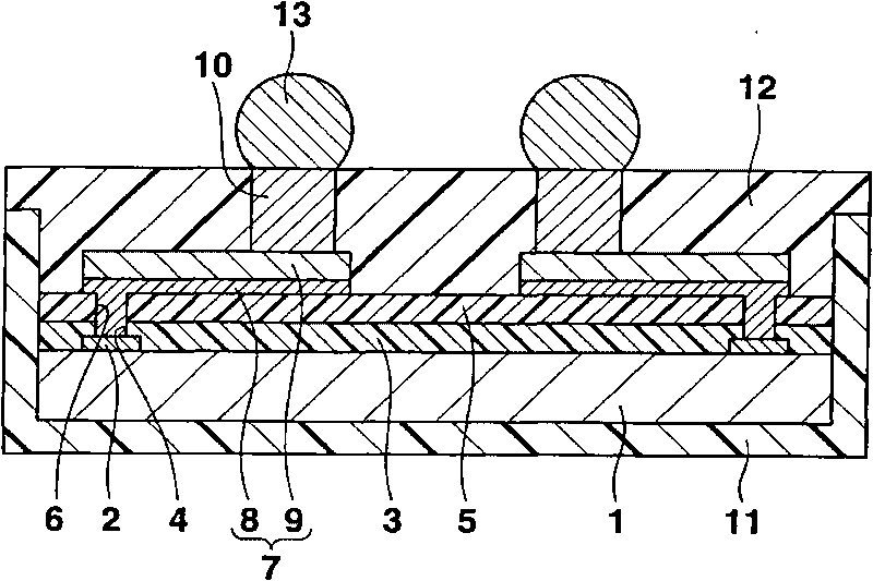
[0024] figure 1 A cross-sectional view showing an example of a semiconductor device manufactured by the manufacturing method of the present invention. This semiconductor device is generally called a CSP, and includes a silicon substrate (semiconductor substrate) 1 . On the upper surface of the silicon substrate 1, elements constituting an integrated circuit with specified functions, such as elements (not shown) such as transistors, diodes, resistors, and capacitors (not shown), are formed. Connection pads 2 made of aluminum-based metal or the like on each element. Only two connection pads 2 are shown in the figure, but actually a plurality of connection pads 2 are arranged on the peripheral portion of the upper surface of the silicon substrate 1 .

[0025] A passivation film (insulating film) made of silicon oxide or the like is provided on the upper surface of the silicon substrate 1 except for the central portion of the connection pad 2, and the central portion of the conn...


PUM


Abstract

First, a trench formed in parts of a semiconductor wafer, a sealing film and others corresponding to a dicing street and both sides thereof. In this state, the semiconductor wafer is separated into silicon substrates by the formation of the trench. Then, a resin protective film is formed on the bottom surface of each silicon substrate including the inner part of the trench. In this case, the semiconductor wafer is separated into the silicon substrates. However, a support plate is affixed to the upper surfaces of the columnar electrode and the sealing film via an adhesive layer. Therefore, when the resin protective film is formed, it is possible to prevent the entirety including the separated silicon substrates from being easily warped.

Description

technical field [0001] The present invention relates to a method of manufacturing a semiconductor device in which the bottom and side surfaces of a semiconductor substrate are covered with a resin protective film. Background technique [0002] In (Japanese) Patent No. 4103896, a so-called CSP (Chip Size Package) is known. In this semiconductor device, a plurality of wirings are provided on the upper surface of an insulating film provided on a semiconductor substrate, columnar electrodes are provided on the upper surface of connection pads of the wirings, and a plurality of wirings are provided on the upper surface of the insulating film including the wirings. A sealing film is provided so that the upper surface is on the same plane as the upper surface of the columnar electrode, and solder balls are provided on the upper surface of the columnar electrode. In this case, the lower surface and side surfaces of the semiconductor substrate are covered with a resin protective fil...

Claims


Application Information

Patent Timeline
Patent Type & Authority Applications(China)
IPC IPC(8): H01L21/50H01L21/56
CPCH01L2224/18H01L23/3114H01L23/3135H01L24/94H01L2924/01047H01L21/78H01L24/03H01L2924/09701H01L2224/16H01L24/13H01L2924/14H01L21/6836H01L24/05H01L2924/01033H01L24/11H01L2924/01006H01L24/19H01L2924/01029H01L2221/6834H01L2924/19041H01L2924/01012H01L21/568H01L2924/01013H01L2224/94H01L2224/0401H01L2924/3511H01L2224/023H01L2224/11H01L2224/03H01L2924/0001H01L23/28
Inventor 小六泰辅冈田修桑原治盐田纯司藤井信充
Owner TERAMIKROS INC
Why Eureka
Try Eureka