Method for depositing film

A technology of thin film and alloy thin film, which is applied in the field of depositing amorphous silicon alloy thin film, can solve the problems of large electrode and glass substrate area, unbalanced and uneven power distribution, etc., to improve uniformity and consistency, and increase process tolerance , the effect of improving efficiency

Inactive Publication Date: 2010-07-14
GS SOLAR FU JIAN COMPANY +1
View PDF4 Cites 21 Cited by
  • Summary
  • Abstract
  • Description
  • Claims
  • Application Information

AI Technical Summary

Problems solved by technology

However, just because the overall volume of the reaction chamber 110 is large, the area of ​​the electrodes and the glass substrate is large, and due to factors such as manufacturing tolerances and use deformation, it is impossible to achieve absolute parallelism between the electrode plates during installation, and the glass substrate The installation is not absolutely parallel, so the areas on both sides of the electrode plate are not completely symmetrical, even if the upper and lower spaces on the same side are not consistent, this asymmetry and inhomogeneity will lead to unbalanced power distribution in each discharge area , unevenness, this phenomenon will become more serious with the reduction of continuous radio frequency output power, when the continuous radio frequency output power is low to a certain value, even one side of the electrode plate will glow and the other side will not glow, Seriously affects the consistency and uniformity of thin film deposition on batch substrates

Method used


Image

  • Method for depositing film
  • Method for depositing film
  • Method for depositing film

Examples


Embodiment Construction

[0032] In order to make the above objects, features and advantages of the present invention more comprehensible, specific implementations of the present invention will be described in detail below in conjunction with the accompanying drawings. In the following description, numerous specific details are set forth in order to provide a thorough understanding of the present invention. However, the present invention can be implemented in many ways other than those described here, and those skilled in the art can make similar extensions without departing from the connotation of the present invention. Accordingly, the invention is not limited to the specific implementations disclosed below.

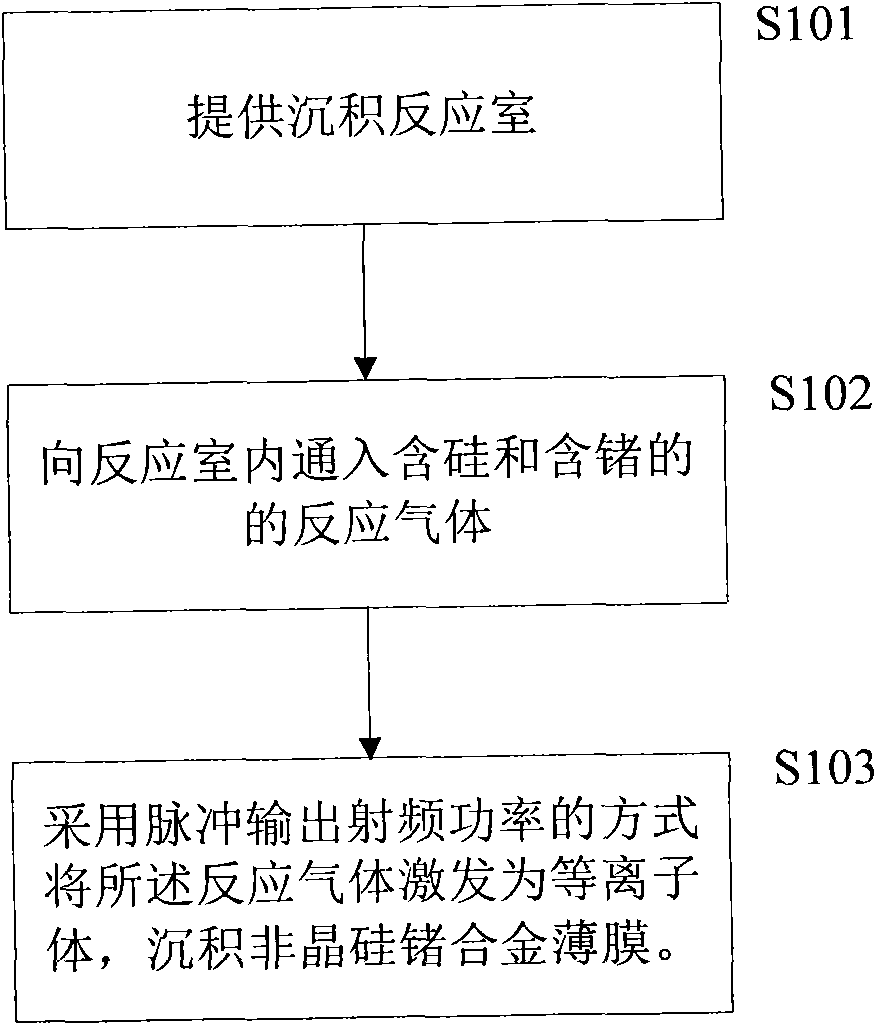
[0033] image 3 It is a flowchart of the first embodiment of the thin film deposition method of the present invention. In this embodiment, the deposition of an amorphous silicon germanium (a-SiGe) alloy thin film is taken as an example. The photoelectric conversion efficiency of silicon-base...


PUM


Abstract

The invention discloses a method for depositing a thin film. The method comprises the following steps of: providing a reaction chamber, wherein a substrate is placed on the surfaces of electrode plates which are alternately placed at intervals in the reaction chamber; leading reaction gas into the reaction chamber; exciting the reaction gas into plasmas by adopting a mode of pulse output radio frequency power; and depositing a thin film on the surface of the substrate. The method can obviously improve the band gap and the thickness uniformity of a thin film and particularly an alloy thin film deposited on the surface of the large-area substrate in large-size PECVD (Plasma Enhanced Chemical Vapor Deposition) deposition equipment.

Description

technical field [0001] The invention relates to the technical field of photovoltaic solar cells, in particular to a method for depositing an amorphous silicon alloy thin film. Background technique [0002] With the increasing shortage of energy, people pay more and more attention to the development and utilization of solar energy. There is an increasing demand for new solar cells with larger areas, lighter and thinner, and lower production costs. Among these new solar cells, the development of silicon-based alloy thin-film solar cells (hereinafter referred to as thin-film solar cells), especially large-area thin-film solar cells, has attracted worldwide attention. Thin-film solar cells use very little silicon, which makes it easier to reduce costs. In the case of continuous shortage of silicon raw materials, thin-film solar cells have become a new trend and new hotspot in the development of solar cells. [0003] Thin film solar cells are multilayer devices such as figure ...

Claims


Application Information

Patent Timeline
Patent Type & Authority Applications(China)
IPC IPC(8): C23C16/50C23C16/30H01L31/18
CPCH01L21/02532C23C16/22Y02E10/50H01L31/204C23C16/515H01L21/0262Y02P70/50
Inventor 李沅民单洪青林朝晖
Owner GS SOLAR FU JIAN COMPANY
Why Eureka
Try Eureka