Solid-state imaging device

一种固体摄像装置、分光的技术,应用在高灵敏度化及包含红外光的彩色化领域,能够解决彩色化欠缺灵活性等问题

Active Publication Date: 2010-07-14
SAMSUNG ELECTRONICS CO LTD
View PDF7 Cites 34 Cited by
  • Summary
  • Abstract
  • Description
  • Claims
  • Application Information

AI Technical Summary

Problems solved by technology

That is, it must be divided into at least three kinds of light of RGB by a diffraction grating, and there is a problem of lack of flexibility in colorization

Method used


Image

  • Solid-state imaging device
  • Solid-state imaging device
  • Solid-state imaging device

Examples


Embodiment approach 1

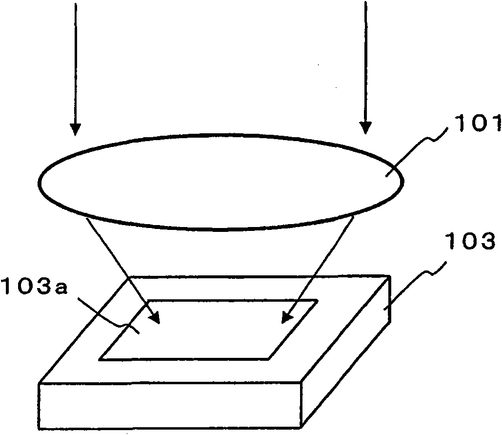
[0131] Figure 1A It is a perspective view schematically showing how light transmitted through the lens 101 enters the solid-state imaging device 103 . On the imaging surface 103 a of the solid-state imaging device 103 , a plurality of photosensitive cells are arranged two-dimensionally. As a result of imaging achieved by the lens 101 , the amount of light incident on the imaging surface 103 a (incident light amount) varies depending on the incident position. Typically, each photosensitive unit is a photodiode, and outputs an electrical signal (photoelectric conversion signal) corresponding to the amount of incident light through photoelectric conversion. Typically, the solid-state imaging element 103 is a CCD or a CMOS sensor, and is manufactured by known semiconductor manufacturing techniques. An array of optical elements having a spectroscopic function is provided at a position facing the surface on which the photosensitive cell array is formed in the solid-state imaging ...

Embodiment approach 2

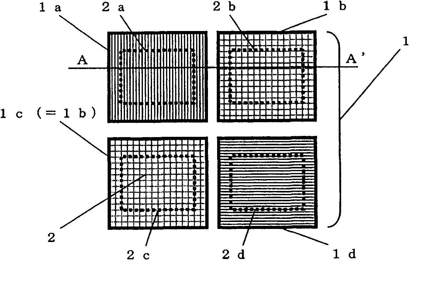
[0161] Next, a second embodiment will be described with reference to the drawings. Figure 2A It is a diagram showing the arrangement of an optical element array in Embodiment 2 of the present invention, and is a plan view of an imaging element basically composed of photosensitive cells in 2 rows and 2 columns. Figure 2B It is a plan view showing the type of light incident on the photosensitive cell.

[0162] The basic configuration of the present embodiment is similar to that of the first embodiment, except that the elements corresponding to the light-splitting elements 1d of the optical element array 1 are replaced with transparent elements 1e.

[0163] The spectroscopic elements 1a and 1b in this embodiment are the same as those of the first embodiment. Therefore, the amount of light received by the photosensitive units 2a, 2b directly below them is also the same as Figure 2B As shown, it is the same as the case of Embodiment 1. Therefore, the color signal 2C2 and the ...

Embodiment approach 3

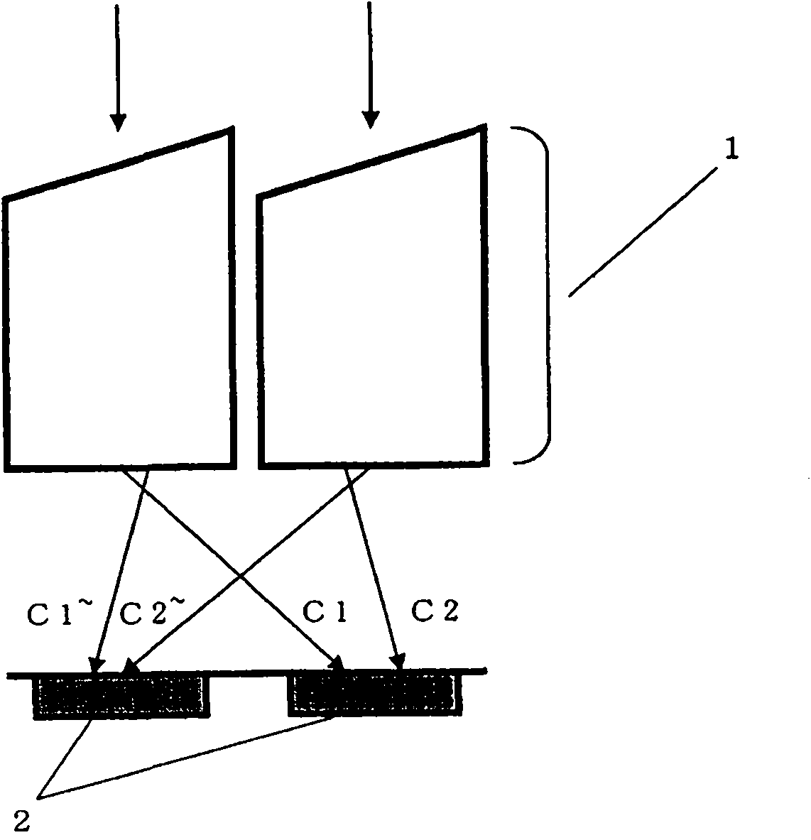
[0169] Next, a third embodiment will be described with reference to the drawings. 3 is a diagram showing the arrangement of an optical element array in Embodiment 3 of the present invention, and is a plan view of an imaging element basically composed of photosensitive cells in 2 rows and 2 columns. Figure 3B It is a plan view showing the type of light incident on the photosensitive cell.

[0170] The basic configuration of the optical element array is similar to that of Embodiment 1, except that the elements corresponding to the light-splitting element 1b and the elements corresponding to the light-splitting element 1c of the optical element array 1 are replaced with simple transparent elements 1e, Also exactly the same. That is, in the basic unit of 2 rows and 2 columns, one transparent element is used in Embodiment 2, and two transparent elements are used in this embodiment.

[0171] In this embodiment, there are two transparent elements 1e, and the light receiving units ...


PUM


Abstract

The device has spectroscopic elements in a basic configuration of two rows and two columns, spectroscopic elements (1a, 1b) and spectroscopic elements (1c, 1d) each form a set, and dispersed light is emitted onto photosensor units and adjoining photosensor cells that are provided directly below them. The light is dispersed such that the spectroscopic element (1a) emits primary color light (C1) to an adjoining cell (2b) while emitting the complementary color light (C1') to the cell (2a) provided directly below it, the spectroscopic element (1b) emits a primary color light (C2) to the cell (2b) provided directly below it while emitting the complementary color light (C2') to an adjoining cell (2a), the spectroscopic element (1c) operates identically to spectroscopic element (1b), and the spectroscopic element (1d) emits a primary color light (C3) to an adjoining cell (2c) while emitting the complementary color light (C3') to the cell (2d) provided directly below it. The photosensor cells (2) output electric signals by means of photoelectric conversion according to the amounts of incident light. A color signal and a brightness signal are generated through simple computation between the outputs of the respective photosensor cells.

Description

technical field [0001] The present invention relates to a technology for increasing the sensitivity of a solid-state imaging device and for coloring infrared light. Background technique [0002] In recent years, digital cameras using solid-state imaging devices such as CCDs and CMOSs ​​(hereinafter sometimes referred to as "imaging elements") and digital cinemas have rapidly advanced in functionality and performance. In particular, advances in semiconductor manufacturing technology have enabled the miniaturization of pixel structures in solid-state imaging devices, enabling high integration of pixels and driving circuits in solid-state imaging devices. Therefore, in just a few years, the number of pixels of the camera element has increased significantly from 1 million pixels to 10 million pixels. However, from another point of view, since the amount of light received by one pixel (light amount) decreases with the increase in the number of pixels of the imaging element, ther...

Claims


Application Information

Patent Timeline
Patent Type & Authority Applications(China)
IPC IPC(8): H01L27/14H04N9/07
CPCH01L27/14621H04N5/2254H01L27/14627H04N9/045H04N5/33H01L27/14629H01L27/14625H04N25/134
Inventor 平本政夫米本和也西胁青儿铃木正明杉谷芳明若林信一
Owner SAMSUNG ELECTRONICS CO LTD
Why Eureka
Try Eureka