
MOS (Metal Oxide Semiconductor) formation method and threshold voltage adjustment method thereof

A MOS transistor and threshold voltage technology, which is applied in the manufacturing of circuits, electrical components, semiconductor/solid-state devices, etc., can solve the problems of complex MOS transistor manufacturing process, and achieve the effect of shortening the process cycle, saving costs, and flexibly adjusting

Active Publication Date: 2010-07-21
SEMICON MFG INT (SHANGHAI) CORP
View PDF0 Cites 9 Cited by
  • Summary
  • Abstract
  • Description
  • Claims
  • Application Information

AI Technical Summary

Problems solved by technology

The most common way is to change the ion implantation type, energy and dose, and to change the thickness of the gate oxide layer, but no matter which method, it is necessary to increase the well (well), so that different masks will be used to define different The device area makes the manufacturing process of the entire MOS transistor more complicated

Method used


Image

  • MOS (Metal Oxide Semiconductor) formation method and threshold voltage adjustment method thereof
  • MOS (Metal Oxide Semiconductor) formation method and threshold voltage adjustment method thereof
  • MOS (Metal Oxide Semiconductor) formation method and threshold voltage adjustment method thereof

Examples


Embodiment Construction

[0038] Although the invention will be described in more detail below with reference to the accompanying drawings, in which preferred embodiments of the invention are shown, it should be understood that those skilled in the art can modify the invention described herein and still achieve the advantageous effects of the invention. Therefore, the following description should be understood as a broad instruction for those skilled in the art, rather than as a limitation of the present invention.

[0039] In the following paragraphs the invention is described more specifically by way of example with reference to the accompanying drawings. Advantages and features of the present invention will become apparent from the following description and claims. It should be noted that the drawings are all in a very simplified form and use imprecise ratios, which are only used to facilitate and clearly assist the purpose of illustrating the embodiments of the present invention.
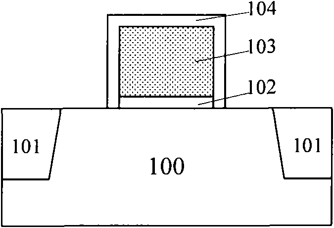
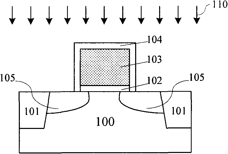
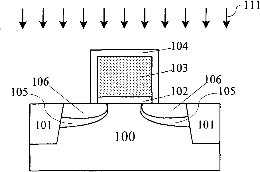
[0040] The step...


PUM

PropertyMeasurementUnit
Thicknessaaaaaaaaaa

Abstract

The invention discloses an MOS (Metal Oxide Semiconductor) formation method and a threshold voltage adjustment method thereof. The MOS formation method comprises the steps of: forming a grid structure on a semiconductor substrate; penetrating the grid structure to carry out second iron injection to form an ion diffusion area for adjusting threshold voltage and a bag shaped injection area; carrying out ion injection at two sides of the grid structure and in the semiconductor substrate to form resource / drain electrode extension areas and resource / drain electrodes; and annealing the semiconductor substrate, wherein the injection quantity and dosage of second ion is determined by the MOS threshold voltage. The method is applicable to the threshold voltage adjustment of long-channel and short-channel components without adding an extra well to separately perform parallel threshold voltage adjustment to components with different size, thereby realizing simple and flexible threshold voltage adjustment, shortening production process cycle, and saving cost.

Description

technical field [0001] The invention relates to the technical field of semiconductor manufacturing, in particular to a method for forming a MOS transistor and a method for adjusting a threshold voltage thereof. Background technique [0002] At present, due to the increasing integration of integrated circuits, the size of devices is getting smaller and smaller, and the feature size (CD) of devices is developed from 0.13 μm to below 0.10 μm. Metal-oxide-semiconductor (MOS) devices are the main driving force as semiconductor devices move toward high density and small size. Threshold voltage (Vt) and drive current (Id) are two important electrical parameters of MOS transistors, and are also important control parameters in the manufacturing process. Different core circuits (Core) and input / output circuits (IO) have different Vt and Id performance requirements. [0003] In the prior art, the doping shape of the gate oxide layer, channel region, well region, source / drain extensio...

Claims


Application Information

Patent Timeline
IPC IPC(8): H01L21/336H01L21/265
Inventor 神兆旭居建华
Owner SEMICON MFG INT (SHANGHAI) CORP
Features
  • Generate Ideas
  • Intellectual Property
  • Life Sciences
  • Materials
  • Tech Scout
  • Unparalleled Data Quality
  • Higher Quality Content
  • 60% Fewer Hallucinations
Learn More