Pixel structure and manufacturing method thereof and manufacturing method of electronic device

A technology of pixel structure and manufacturing method, which is applied in the manufacture of electronic devices, pixel structure and its manufacturing field, can solve problems such as pixel structure degradation, and achieve the effect of solving degradation problems and good component characteristics

Active Publication Date: 2010-07-28
AU OPTRONICS CORP
View PDF4 Cites 14 Cited by
  • Summary
  • Abstract
  • Description
  • Claims
  • Application Information

AI Technical Summary

Problems solved by technology

[0005] The invention provides a pixel structure to solve the problem of deterioration of the pixel structure under ultraviolet light irradiation

Method used


Image

  • Pixel structure and manufacturing method thereof and manufacturing method of electronic device
  • Pixel structure and manufacturing method thereof and manufacturing method of electronic device
  • Pixel structure and manufacturing method thereof and manufacturing method of electronic device

Examples


Embodiment Construction

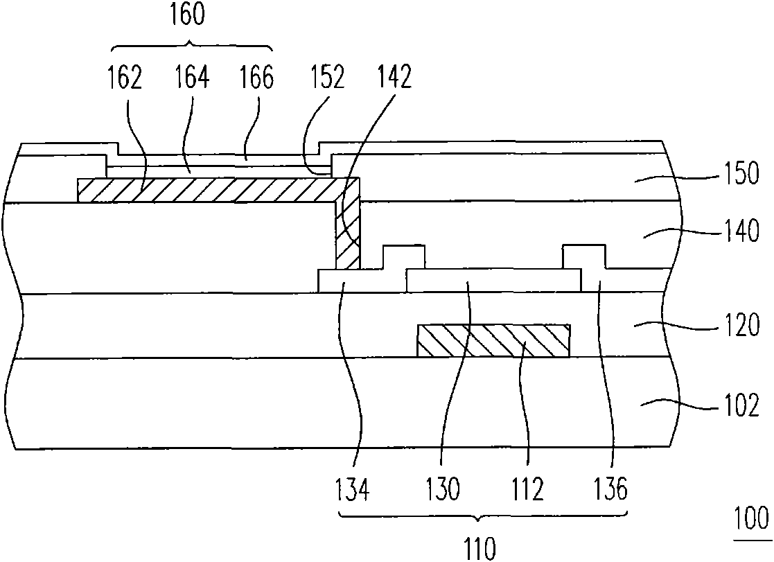
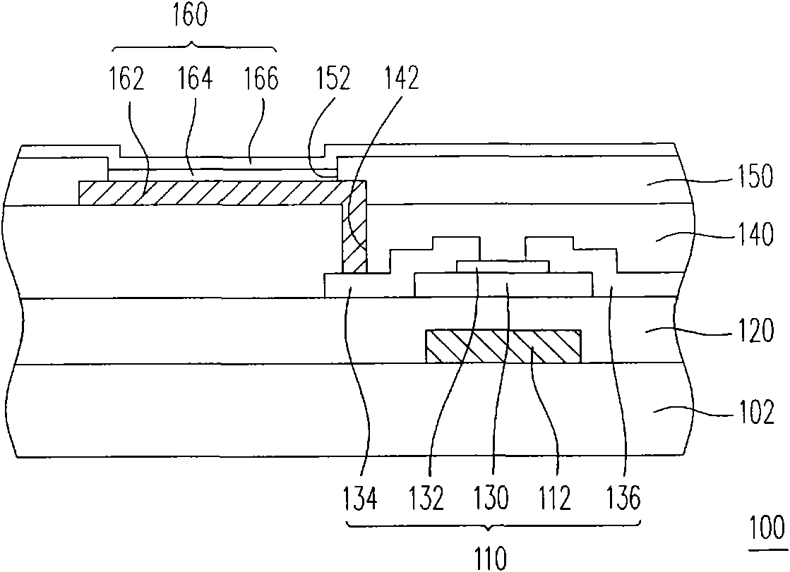
[0036] figure 1 It is a schematic cross-sectional view of a pixel structure according to an embodiment of the present invention. Please refer to figure 1 The pixel structure 100 includes a substrate 102 , a gate 112 , an insulating layer 120 , a metal oxide semiconductor layer 130 , a source 134 and a drain 136 , a first protection layer 140 and a first electrode layer 162 . Wherein, the gate 112 , the metal oxide semiconductor layer 130 , the source 134 and the drain 136 constitute the active device 110 . In detail, the gate 112 is located on the substrate 102 . The insulating layer 120 covers the gate 112 . The metal oxide semiconductor layer 130 is on the insulating layer 120 above the gate 112 . The source 134 and the drain 136 are located on the metal oxide semiconductor layer 130 . The first passivation layer 140 is located on the source electrode 134 and the drain electrode 136 and covers the metal oxide semiconductor layer 130 . In this embodiment, the metal oxid...


PUM

PropertyMeasurementUnit
wavelengthaaaaaaaaaa

Abstract

The invention discloses a pixel structure, comprising a substrate, a grid, an insulating layer, a metal oxide semiconductor layer, a source, a drain, at least a film layer and a first electrode layer, wherein the grid is positioned on the substrate; the insulating layer covers the grid; the metal oxide semiconductor layer is positioned on the insulating layer above the grid; the source and the drain are positioned on the metal oxide semiconductor layer; the film layer covers the metal oxide semiconductor layer and comprises a transparent photocatalyst material which blocks the light in the ultraviolet light band from penetrating through the metal oxide semiconductor layer; and the first electrode layer is electrically connected with the source or the drain. The invention simultaneously discloses a manufacturing method of the pixel structure and a manufacturing method of an electronic device.

Description

technical field [0001] The present invention relates to a pixel structure, and in particular to a pixel structure, a manufacturing method thereof, and a manufacturing method of an electronic device with the pixel structure. Background technique [0002] An electroluminescence device is a self-luminous (Emissive) device. Because the electroluminescent device has no viewing angle limitation, low manufacturing cost, high response speed (about a hundred times higher than that of liquid crystal), power saving, DC drive that can be used in portable machines, wide operating temperature range, light weight and portable The advantages of miniaturization and thinning of hardware equipment, etc. Therefore, electroluminescent devices have great potential for development and are expected to become novel flat panel displays of the next generation. [0003] Taking the active electroluminescent device as an example, it includes a plurality of pixel structures, and the pixel structure incl...

Claims


Application Information

Patent Timeline
Patent Type & Authority Applications(China)
IPC IPC(8): H01L27/32H01L27/15H01L21/82H01L21/316H01L21/56
Inventor 周政伟吕学兴丁宏哲石宗祥陈佳榆
Owner AU OPTRONICS CORP
Why Eureka
Try Eureka