Method for manufacturing PCB (printed circuit board), PCB and device

A technology for printed circuit boards and sub-boards, which is applied in the direction of assembling printed circuits with electrical components, printed circuits connected with non-printed electrical components, printed circuit components, etc., which can solve technical difficulties and limited application scenarios, etc. Problems, to achieve the effect of increasing layout density and applying a wide range of scenarios

Active Publication Date: 2010-07-28
HUAWEI TECH CO LTD
View PDF0 Cites 11 Cited by
  • Summary
  • Abstract
  • Description
  • Claims
  • Application Information

AI Technical Summary

Problems solved by technology

[0003] During the research and practice of the prior art, the inventor of the present invention found that since the pins of the two press-fit connectors are in the same through hole, for pins with different attributes, signal isolation needs to be carried out in the middle , that is, it needs to be isolated in the middle of the through hole, and it is difficult to realize this in the process. Limited (generally used for pressure against grounded enclosures, such as shielded enclosures)

Method used


Image

  • Method for manufacturing PCB (printed circuit board), PCB and device
  • Method for manufacturing PCB (printed circuit board), PCB and device
  • Method for manufacturing PCB (printed circuit board), PCB and device

Examples


Embodiment 1

[0023] An embodiment of the present invention provides a printed circuit board. Embodiments of the present invention also provide a corresponding printed circuit board device assembled with a connector, and a method for manufacturing the printed circuit board. Each will be described in detail below.

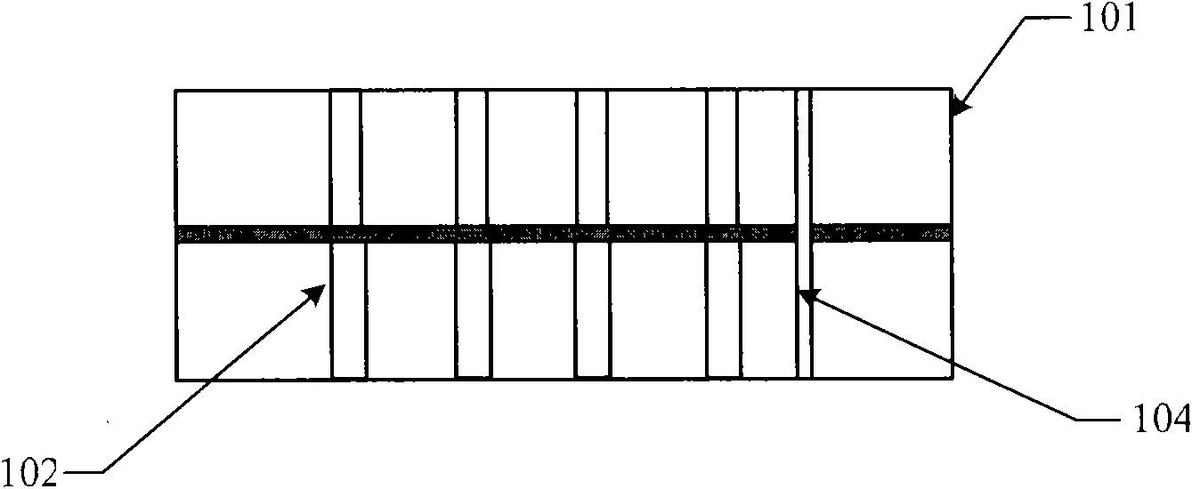
[0024] A printed circuit board has blind holes on both sides, and the blind holes are used to press the pins of the connectors, so as to realize the pressing of the connectors on the two sides of the printed circuit board.

[0025] Since the holes on the printed circuit board used to press into the connector pins, that is, the crimping holes of the connector are blind holes, not only the pressure of the connectors on both sides of the printed circuit board can be realized, but also the connector pins can be realized. The signal isolation between them saves the layout space of the printed circuit board.

[0026] The printed circuit board can also have a via hole, which is used t...

Embodiment 2

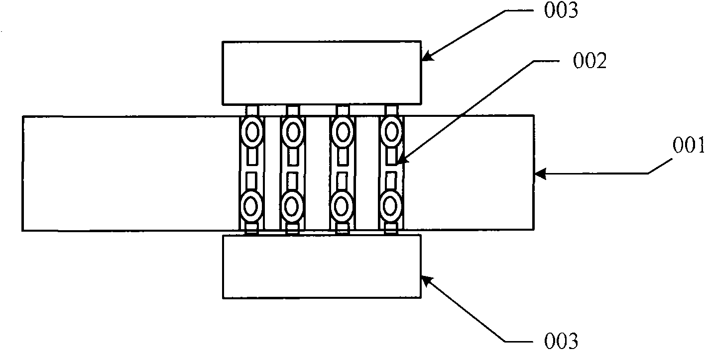
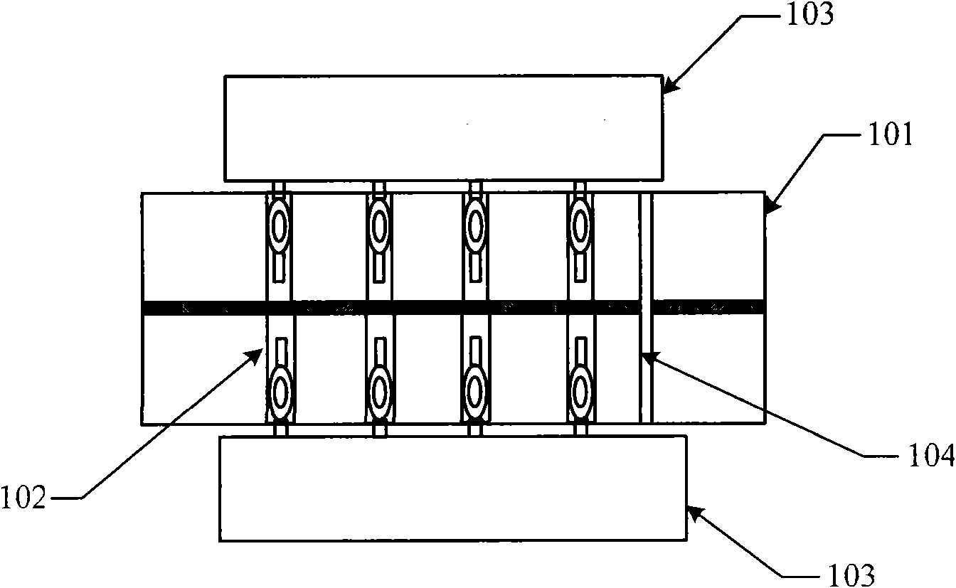
[0041] Correspondingly, the embodiment of the present invention also provides a printed circuit board device assembled with a connector, such as Figure 3 to Figure 7 As shown, the printed circuit board device assembled with a connector may include a connector 103 and any printed circuit board 101 provided by the embodiment of the present invention (see Embodiment 1 for details);

[0042] Both sides of the printed circuit board 101 have blind holes 102, and at least one pin of the connector 103 is pressed into the blind hole 102, so as to realize the opposite pressure with the connector 103 located on the other side of the printed circuit board 101. . Since the holes on the printed circuit board used to press into the connector pins, that is, the crimping holes of the connector are blind holes, not only the pressure of the connectors on both sides of the printed circuit board can be realized, but also the connector pins can be realized. The signal isolation between them saves...


PUM


Abstract

The invention discloses a method for manufacturing a PCB (printed circuit board), a PCB and a device. Blind holes are respectively arranged on the two surfaces of the PCB provided by the embodiment of the invention, and are used for pressing in pins of connectors so as to realize opposite pressing of the connectors arranged on the two surfaces of the PCB. The blind holes are adopted to avoid the problem of mutual signal interference due to that two pins with different attributes are located in the same hole when in opposite pressing; namely, the scheme provided by the embodiment of the invention has requirements neither for the attributes of the pins of the connectors nor for the layout of the connectors on the two surfaces of the PCB, thereby not only improving the layout density of the connectors on the PCB, but also creating wide application range.

Description

technical field [0001] The invention relates to the technical field of printed circuit boards, in particular to a method for manufacturing a printed circuit board, a printed circuit board and a device. Background technique [0002] The middle printed circuit board (PCB, Printed Circuit Board) refers to a printed circuit board that can be assembled with connectors on both sides (upper surface and lower surface), and can be inserted into a single board to realize signal connection. Among them, because the middle printed circuit board ( Both the front and rear sides (upper and lower surfaces) of the printed circuit board (hereinafter referred to as the printed circuit board) need to be crimped. , there will be no more connectors at the corresponding positions on the other side of the printed circuit board. However, as the integration of printed circuit boards becomes higher and higher, the connectors that need to be crimped become denser and denser, and the number of traces al...

Claims


Application Information

Patent Timeline
Patent Type & Authority Applications(China)
IPC IPC(8): H05K1/02H05K1/11H05K1/18H05K3/30H01R12/04
Inventor 李志海李敬科张磊欧康华王辉范路平
Owner HUAWEI TECH CO LTD
Why Eureka
Try Eureka