Interlayer member used for producing multilayer wiring board and method of producing the same

a multi-layer wiring board and interlayer member technology, applied in the direction of printed element electric connection formation, physical therapy, massage, etc., can solve the problems of low production cost of metal plates with a three-layer structure, difficult to increase layout density, side etching, etc., to reduce the amount of metal layers to be used, reduce production cost, and easy production

Inactive Publication Date: 2005-10-13
INVENSAS CORP
View PDF7 Cites 8 Cited by
  • Summary
  • Abstract
  • Description
  • Claims
  • Application Information

AI Technical Summary

Benefits of technology

[0062] In addition, the resin layer is placed on the lower surface of the metal layer, and a mechanical strength necessary for the carrier layer can be obtained by means of the resin layer. Therefore, the metal layer can be thin, and hence the amount of the metal layer to be used can be reduced.
[0063] According to the method of producing an interlayer member used for producing a multilayer wiring board according to the sixteenth aspect of the present invention, an etching prevention film for preventing etching of the metal columns for interlayer connection is formed on the upper surface of the carrier layer after the mask film or the interlayer insulating layer is formed and before the metal columns for interlayer connection are formed. Therefore, the etching prevention film can prevent the metal columns for interlayer connection from being etched at the time of removal of the carrier layer.
[0064] Therefore, the carrier layer can be removed without etching the lower surface of the metal column for inter

Problems solved by technology

However, a technique of producing a multilayer wiring board without the use of such a metal plate with a three-layer structure has been developed partly because the production cost of a metal plate with a three-layer structure is expensive.
. . , so it has been difficult to increase a layout density.
. . is performed by the selective etching of the metal fo

Method used


Image

  • Interlayer member used for producing multilayer wiring board and method of producing the same
  • Interlayer member used for producing multilayer wiring board and method of producing the same
  • Interlayer member used for producing multilayer wiring board and method of producing the same

Examples


example 1

[0089] Hereinafter, the present invention will be described in detail by way of examples shown in the figures.

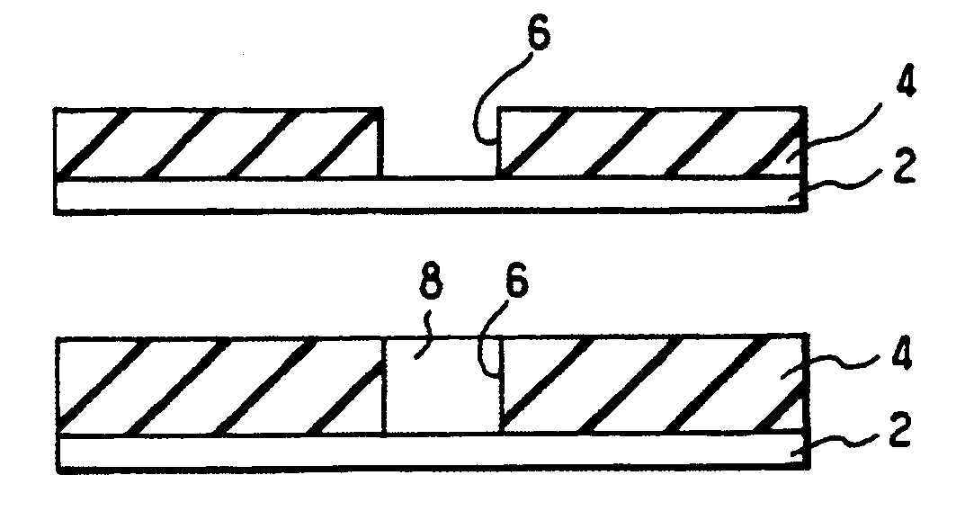
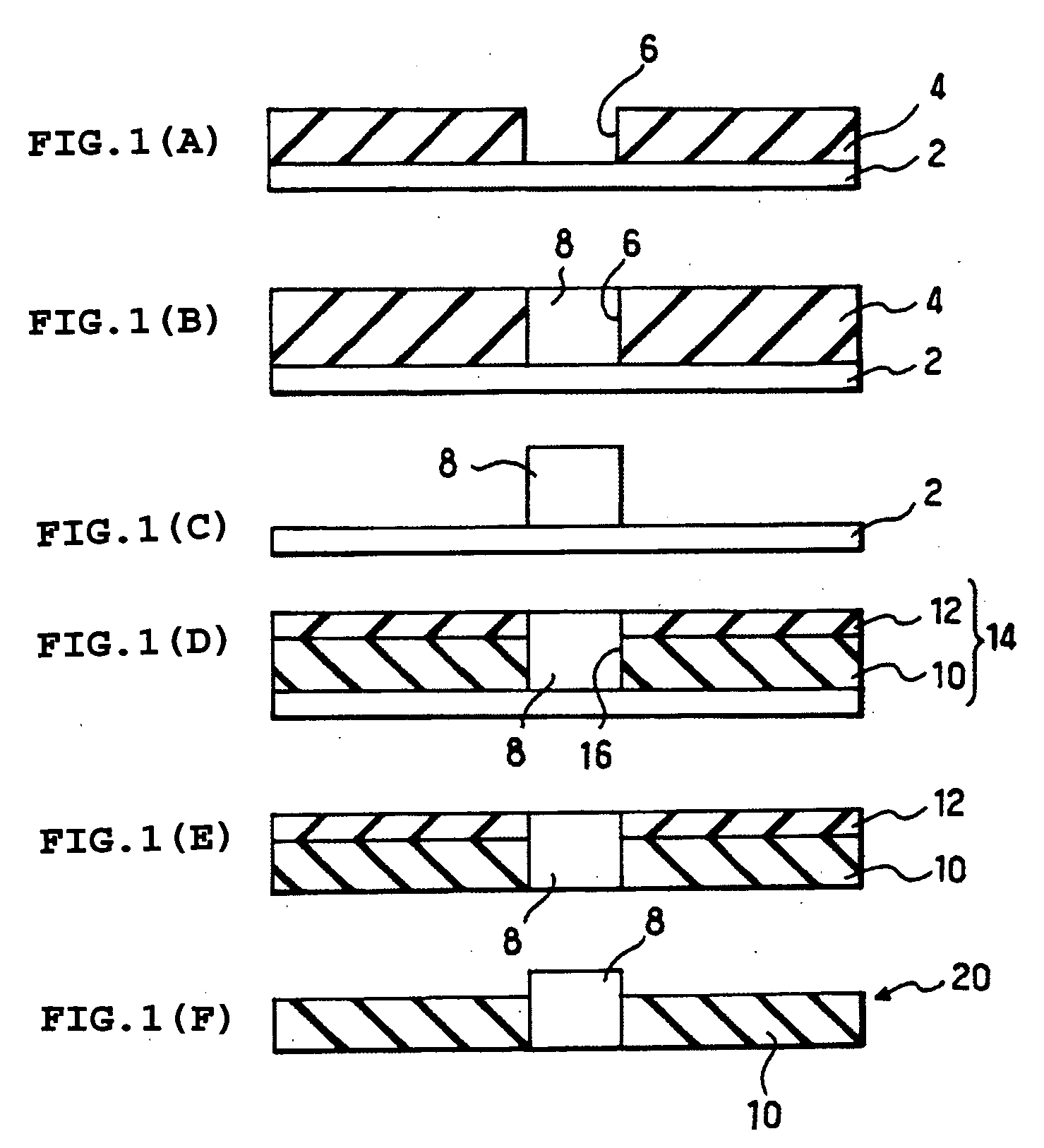
[0090] FIGS. 1(A) to 1(F) are sectional diagrams showing a method of producing an interlayer member used for producing a multilayer wiring board according to Example 1 of the present invention in step order.

[0091] (A) First, a sheet-like carrier layer 2 (having a thickness of, for example, several micrometers to several hundreds of micrometers) made of, for example, copper is prepared. A photosensitive mask film 4 is applied to and formed on the surface of the carrier layer 2. After that, the photosensitive mask film 4 is subjected to exposure and development treatment to produce a mask film having a negative pattern for a large number of metal columns for interlayer connection (8, 8, . . . ) to be formed. FIG. 1(A) shows a state after the exposure and the development treatment. Reference numerals 76, 6, . . . each denotes a hole for interlayer connection of the mask film ...

example 2

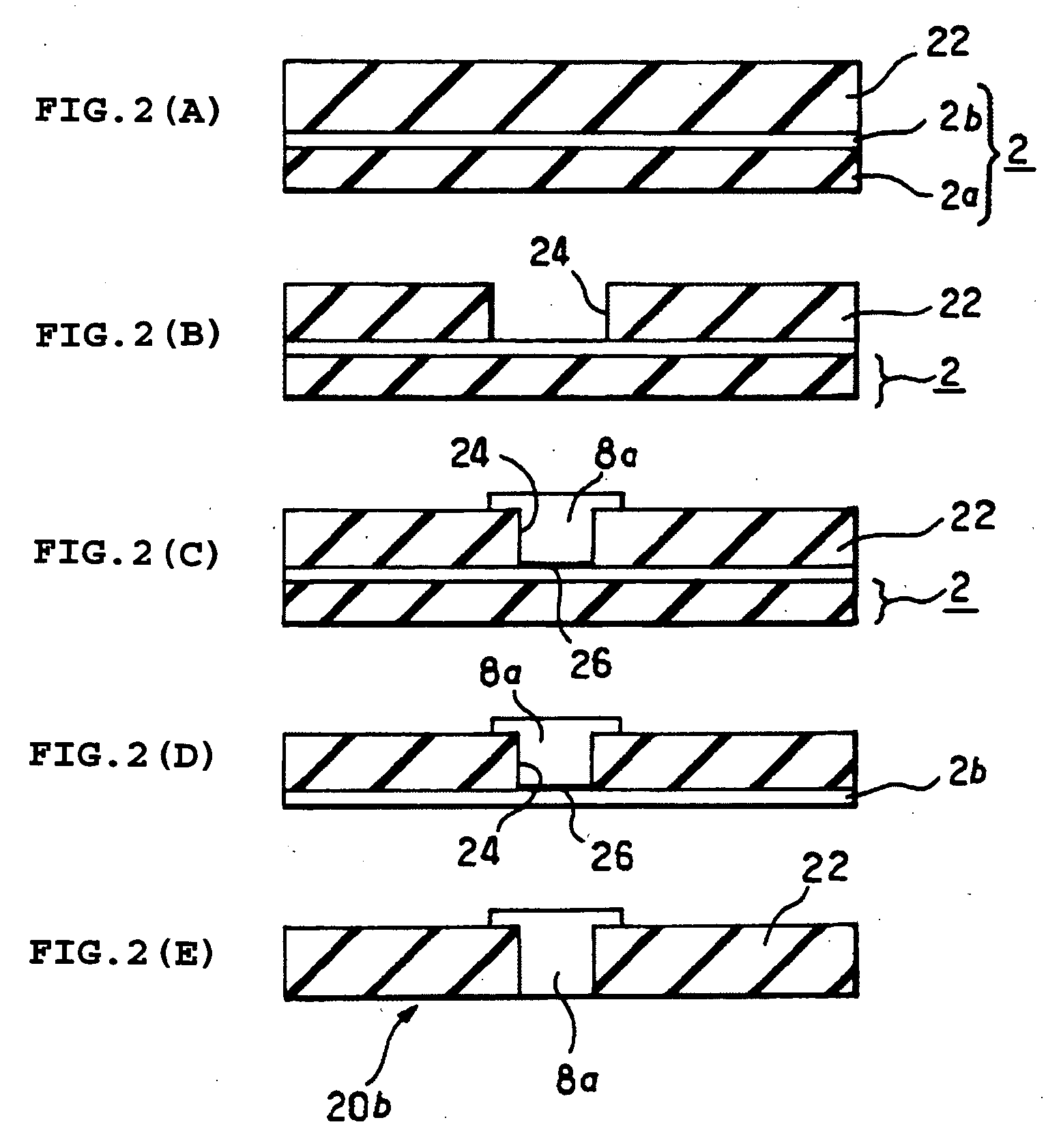
[0102] FIGS. 2(A) to 2(E) are sectional diagrams showing a method of producing an interlayer member used for producing a multilayer wiring board according to Example 2 of the present invention in step order.

[0103] (A) First, a carrier layer 2 made of resin coated copper (RCC) is prepared. An interlayer insulating layer 22 made of, for example, thermoplastic polyimide is formed on the surface of the carrier layer 2. FIG. 2(A) shows a state after the interlayer insulating layer 22 has been formed.

[0104] A photosensitive one may be used as the interlayer insulating layer 22. In this case, the formation of holes for interlayer connection (24, 24, . . . ) to be performed later can be performed by exposure and development.

[0105] Reference symbol 2a denotes a resin film constituting a lower layer of the carrier layer 2. The resin film has a thickness necessary for ensuring the mechanical strength of the carrier layer 2 necessary for ensuring the ease of production, for example, a thickn...

example 3

[0116] FIGS. 3(A) to 3(D) are sectional diagrams showing a method of producing an interlayer member used for producing a multilayer wiring board according to Example 3 of the present invention in step order.

[0117] (A) First, a releasable metal layer 2c (having a thickness of, for example, 2 μm to 6 μm) made of stainless steel (SUS), nickel, or the like is laminated on the upper surface of a resin film 2a. Furthermore, the surface of the releasable metal layer 2c is subjected to potassium permanganate treatment (this treatment is not indispensable) to prepare a carrier layer 2. Then, an interlayer insulating layer 22 made of, for example, thermoplastic polyimide is formed on the surface of the carrier layer 2. FIG. 3(A) shows a state where the interlayer insulating layer 22 has been formed.

[0118] Any one of various metals other than stainless steel and nickel can be used for the releasable metal layer 2c to be laminated on the upper surface of the resin film 2a. For example, a prod...


PUM


Abstract

To increase the dimensional accuracy of an interlayer member used for producing a multilayer wiring board which is inserted between two wiring layers to establish interlayer insulation and interlayer electrical connection between the wiring layers, to thereby increase a layout density. A mask film is formed on a main surface of a sheet-like carrier layer. A metal column for interlayer connection is formed on the main surface of the carrier layer by plating a copper using the mask film as a mask. The mask film is removed. An interlayer insulating layer and a protective sheet are laminated on the main surface of the carrier layer in such a manner that the metal column for interlayer connection penetrates them. The interlayer insulating layer and the protective sheet are polished until the upper surface of the metal column for interlayer connection is exposed. Then, the carrier layer is removed. Furthermore, the protective sheet is removed.

Description

BACKGROUND OF THE INVENTION [0001] 1. Field of the Invention [0002] The present invention relates to an interlayer member used for producing a multilayer wiring board by being inserted between two wiring layers to establish interlayer insulation and interlayer electrical connection between the wiring layers, and to a method of producing the same. [0003] 2. Description of the Related Art [0004] The applicant of the present application has made various propositions in, for example, Japanese Patent Application No. 11-289277 (JP 2001-111189 A) and Japanese Patent Application No. 2003-132793 for a multilayer wiring board using a bump made of a metal such as copper as an interlayer connection means and for a method of producing the same. [0005] Most of the techniques each employ a metal plate with a three-layer structure obtained by: placing an etching barrier layer (having a thickness of, for example, 1 μm) made of, for example, nickel on one surface of a metal layer (having a thickness ...

Claims


Application Information

Patent Timeline
IPC IPC(8): H01L21/4763H01L21/48H01L21/60H01L23/50H05K1/11H05K1/16H05K3/40H05K3/42H05K3/46
CPCH05K3/423H05K3/4614H05K3/4647H05K2201/0355H05K2201/10378H05K2203/0384H05K2203/0726H05K2203/0733H05K2203/1152H01L2924/0002H01L2924/00A61H7/004A61H2201/1692A61H2207/00
Inventor OSAWA, KENJIOSAWA, MASAYUKISHIMADA, TOMOKAZUENDO, KIMITAKAIIJIMA, TOMOO
Owner INVENSAS CORP
Why Eureka
Try Eureka