Chip image collecting and locating device based on rotary reflector

An image acquisition and positioning device technology, applied in the direction of using optical devices, measuring devices, installation, etc., can solve the problems of automatic focusing, image distortion, low chip mounting efficiency, etc., and achieves improved chip mounting efficiency and simple structure. , the effect of continuous chip placement operations

Inactive Publication Date: 2010-08-04
HARBIN INST OF TECH
View PDF5 Cites 23 Cited by
  • Summary
  • Abstract
  • Description
  • Claims
  • Application Information

AI Technical Summary

Problems solved by technology

[0004] The purpose of the present invention is to solve the acquisition of the existing chip moving image using the single-mirror method, the double-mirror method and the half-mirror method, all of which will cause image distortion, require automatic focus, and image distortion. At the same time, the chip In the process of moving to the designated patch position according to a certain path, it needs to stop once in the middle, which leads to the problem of low work efficiency of chip placement. A chip image acquisition and positioning device based on a rotating mirror is provided.

Method used


Image

  • Chip image collecting and locating device based on rotary reflector
  • Chip image collecting and locating device based on rotary reflector
  • Chip image collecting and locating device based on rotary reflector

Examples


specific Embodiment approach 1

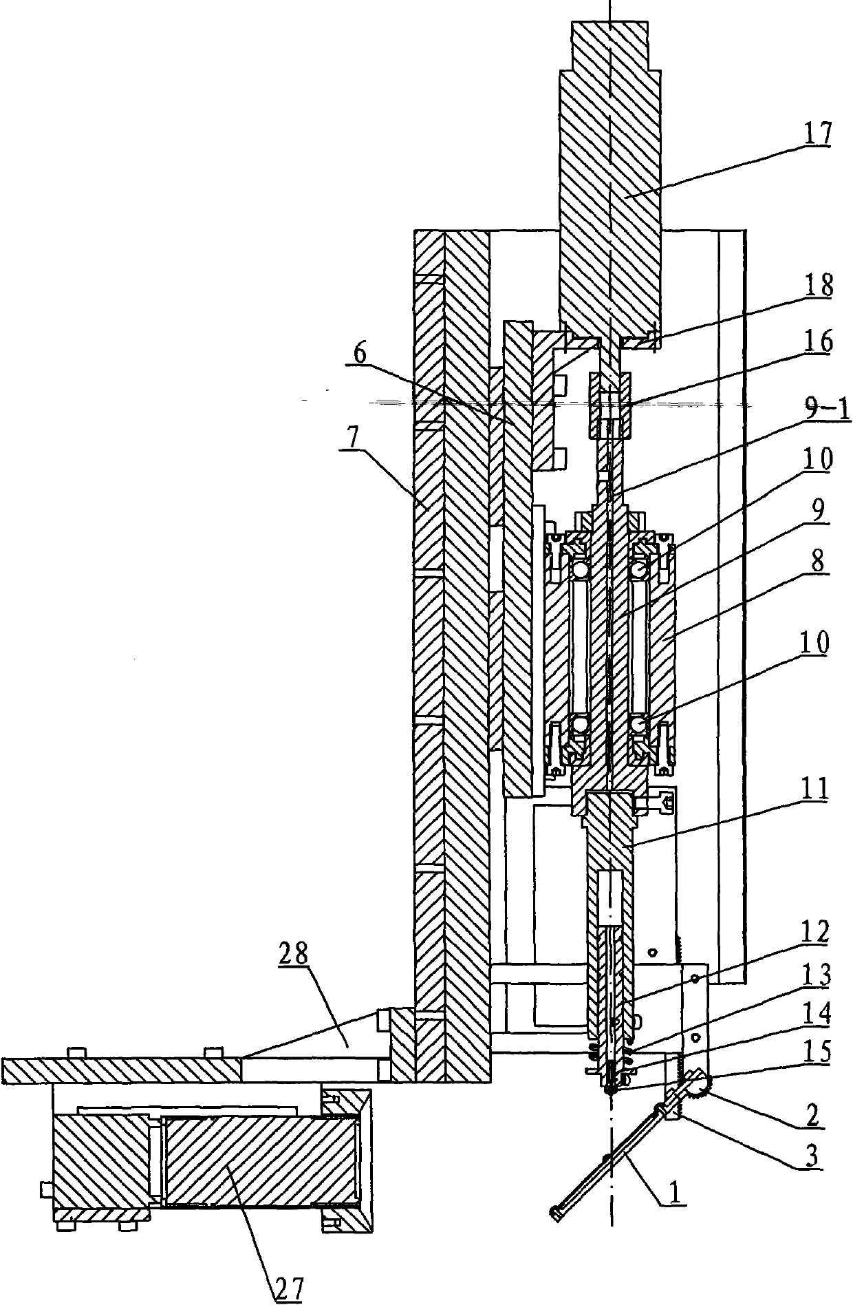
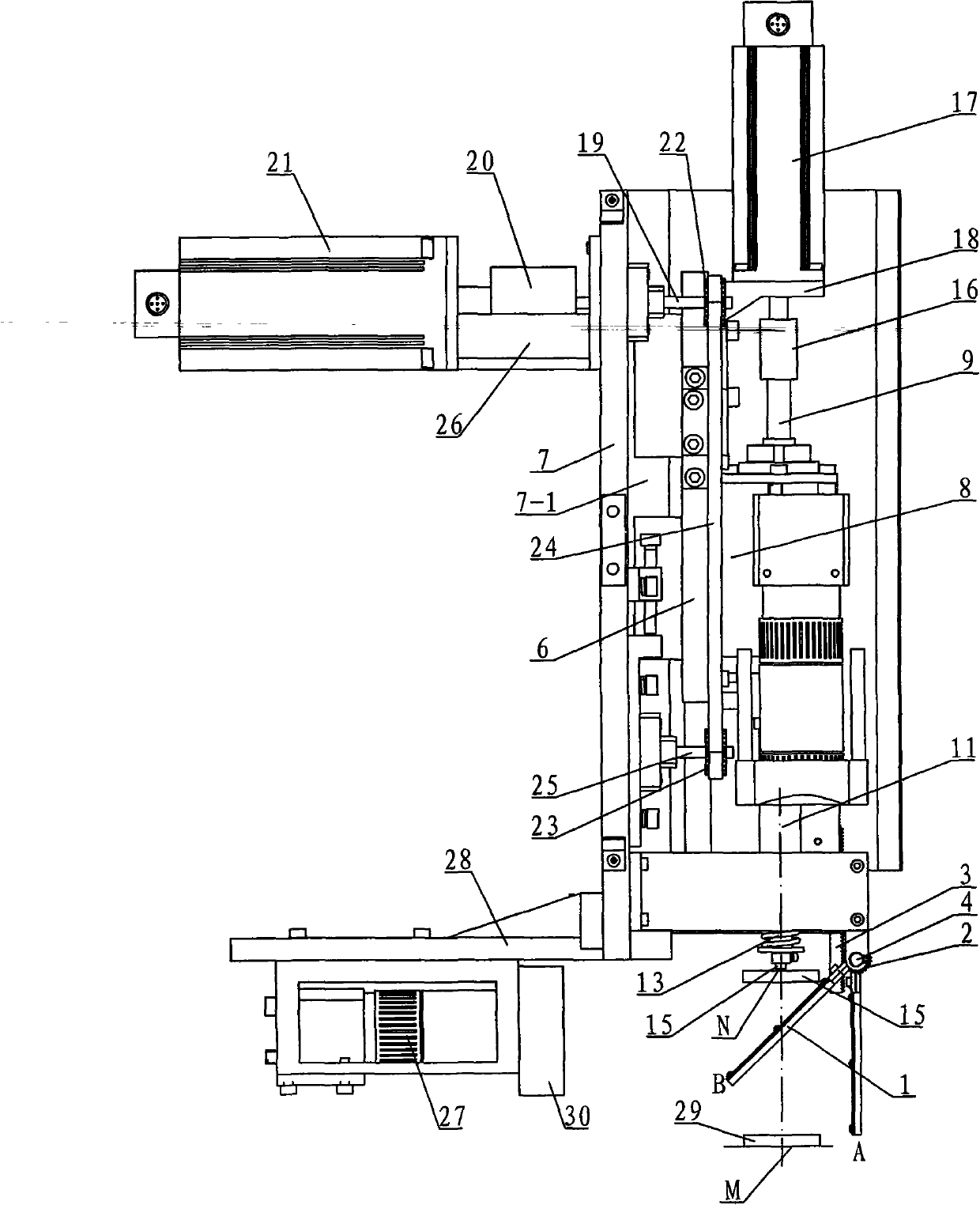
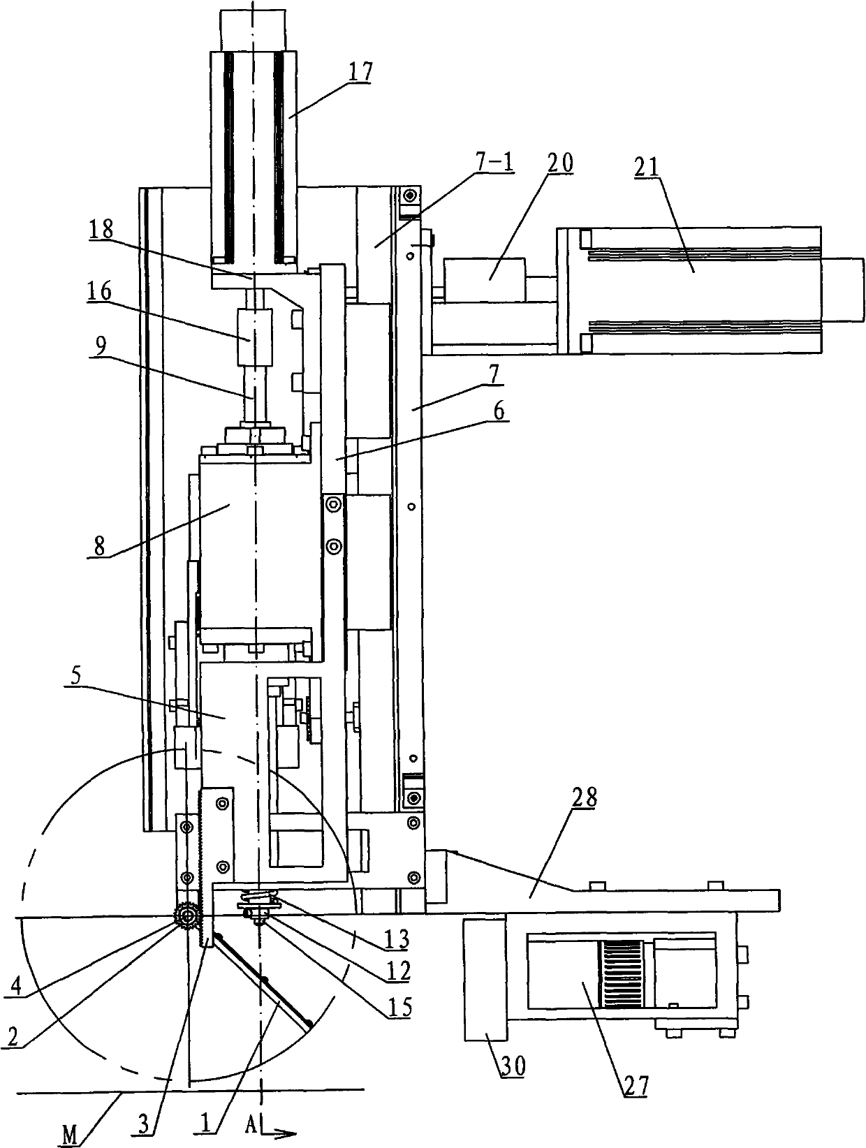
[0008] Specific implementation mode one: combine Figure 1 ~ Figure 3 Describe this embodiment, this embodiment includes a reflector assembly 1, a gear 2, a rack 3, a rotating shaft 4, a support plate 5, a moving base 6, a frame 7, a nozzle sleeve 8, a transmission shaft 9, and two ball bearings 10. Suction nozzle shaft 11, suction nozzle sleeve rod 12, spring 13, suction nozzle rod 14, suction nozzle 15, first coupling 16, rotating motor 17, rotating motor seat 18, upper synchronous belt shaft 19, second coupling Shaft device 20, moving motor 21, upper synchronous belt pulley 22, lower synchronous belt pulley 23, synchronous belt 24, lower synchronous belt shaft 25, motor support 26, camera 27, camera support 28 and light source 30, establish on frame 7 There are guide rails 7-1, the mobile base 6 is installed on the frame 7, the mobile base 6 moves up and down along the frame 7, the suction nozzle sleeve 8 is fixedly connected with the mobile base 6, and the transmission sha...

specific Embodiment approach 2

[0009] Specific implementation mode two: combination Figure 4 Describe this embodiment, the reflector assembly 1 of this embodiment is made up of reflector base plate 1-1 and reflector 1-2, the upper end surface of reflector base plate 1-1 is provided with reflector groove 1-1-1, reflector 1-2 is contained in the reflector groove 1-1-1. Other components and connections are the same as those in the first embodiment.

specific Embodiment approach 3

[0010] Specific implementation mode three: combination Figure 5 The present embodiment will be described. The gear 2 of the present embodiment is a sector gear, and the angle α between the two side faces of the sector gear is 60-70°. This design makes the mirror assembly 1 rotate within the range of 0-45° with the vertical plane, so that the camera 27 can acquire the moving image of the chip when the mirror assembly 1 is at 45° with the vertical plane. Other compositions and connections are the same as those in Embodiment 1 or 2.

[0011] How it works: When die attaching, see figure 2 , the chip 29 is placed in the M position, at this moment, the reflector assembly 1 is parallel to the rack 3 (the position of the reflector assembly 1 is located as figure 2 point A), start the mobile motor 21, the upper synchronous belt shaft 19 drives the upper synchronous belt pulley 22 to rotate, the synchronous belt 24 rotates accordingly, the suction nozzle sleeve 8 and the mobile bas...


PUM


Abstract

The invention discloses a chip image collecting and locating device based on a rotary reflector, relating to an image collection device. The invention aims to solve the problems that image distortion and image deformation occur in the traditional chip motion image collection process, and the chip stops once in the process of moving to an appointed patching position based on a certain path to cause low work efficiency of mounting the chip. When the chip is mounted, a suction nozzle moves downwards firstly to an M position to suck the chip; a mobile motor reversely rotates, the suction nozzle carries the chip to move upwards to an N position, a mobile base drives a rack to move upwards when moving upwards, a gear drives a reflector component to rotate, the lateral end of the reflector component rotates from a point A to a point B, lights of a light source shines on the reflector, a camera obtains a static image of the chip through the reflector, the image is treated by a computer, and the position error of the chip relative to a center coordinate system of the suction nozzle is obtained; and the motor is started to rotate, the suction nozzle rotates, and correction of chip angle error is finished. The invention is used for mounting the chip.

Description

technical field [0001] The invention relates to an image acquisition device. Background technique [0002] In modern electronic manufacturing equipment, the volume of chips is becoming smaller and the degree of chip integration is increasing. It is difficult to achieve high-precision positioning by using traditional operations such as mechanical clamping for chip integration. Therefore, the precision positioning of electronic components and installation stations requires This is done by acquiring images of the component in motion. In the process of electronic manufacturing, the chip integration operation generally uses the suction nozzle to pick up the chip components, and then moves to the designated placement position according to a certain path to perform the placement operation. The nozzle center coordinate system will produce a position error, which includes Δx, Δy, Δθ, where Δx is the X-axis error between the chip center and the nozzle center; Δy is the Y-axis between...

Claims


Application Information

Patent Timeline
Patent Type & Authority Applications(China)
IPC IPC(8): G02B7/198G01B11/03H05K13/04
Inventor 陈立国朱吉锋刘殿冬荣伟彬孙立宁
Owner HARBIN INST OF TECH
Why Eureka
Try Eureka