Semiconductor package and manufacturing method thereof

A manufacturing method, semiconductor technology, applied in the direction of semiconductor devices, semiconductor/solid-state device components, manufacturing tools, etc., can solve problems such as incompatibility and redundant design work

Inactive Publication Date: 2010-08-18
ADVANCED SEMICON ENG INC
View PDF2 Cites 5 Cited by
  • Summary
  • Abstract
  • Description
  • Claims
  • Application Information

AI Technical Summary

Problems solved by technology

Conventionally, additional shielding plates or additional metal layers may be used in prior art, which may not be compatible with complex packaging processes or cause redundant design effort

Method used


Image

  • Semiconductor package and manufacturing method thereof
  • Semiconductor package and manufacturing method thereof
  • Semiconductor package and manufacturing method thereof

Examples


Embodiment Construction

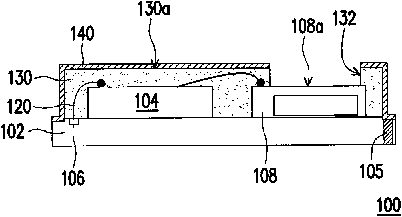
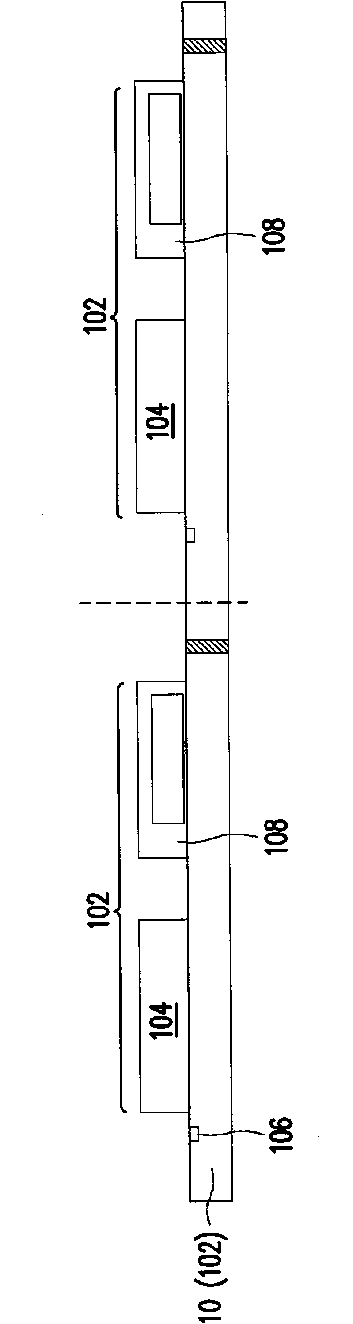
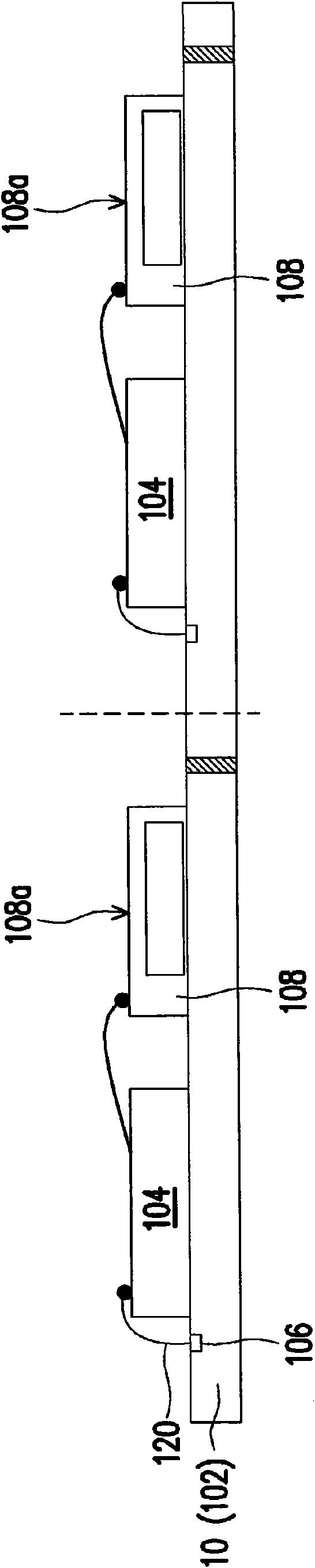
[0027] figure 1 It is a cross-sectional view of a semiconductor package according to a preferred embodiment of the present invention. Please refer to figure 1 , the semiconductor package 100 in this embodiment includes a carrier 102 , at least one chip 104 , at least one contact 106 , at least one sensing element 108 , a plurality of wires 120 , a molding compound 130 and a shielding layer 140 . The carrier 102 may be a laminated semiconductor substrate (eg, a laminated printed circuit board (PCB)) or a leadframe. The sensing element 108 is, for example, an acoustic wave sensing element capable of detecting or sensing sound waves. Preferably, the acoustic wave sensing element can be a MEMS microphone. The sensing element 108 can be electrically connected to the chip 104 via the wire 120 , and the chip 104 is electrically connected to the contact 106 of the carrier 102 via the wire 120 . For example, the material of the shielding layer 140 may be solder material or metal ma...


PUM


Abstract

A semiconductor package including at least a sensing component and a shielding layer is provided. While the shielding layer disposed over the molding compound can protect the semiconductor package from EMI radiations, the sensing component of the package is not blocked by the shielding layer for the feasibility of receiving the sensing signal.

Description

technical field [0001] The present invention relates to a semiconductor package, in particular to a semiconductor package with a sensing component. Background technique [0002] For most electronic devices or packages, electro-magnetic interference (EMI) is a ubiquitous but disturbing disturbance that interrupts, hinders, degrades or limits the effective performance of an electronic device or an entire circuit. Especially, for micro-electro-mechanical system (MEMS) packaging, different mechanical components or elements are combined with various electronic devices, which may even aggravate electromagnetic interference. [0003] In addition, due to the complexity of MEMS packaging, even better EMI shielding must be balanced with the packaging requirements of other mechanical components or devices. Conventionally, additional shielding plates or additional metal layers may be used in the prior art, which may not be compatible with complex packaging processes or cause redundant ...

Claims


Application Information

Patent Timeline
Patent Type & Authority Applications(China)
IPC IPC(8): B81B7/00B81C3/00
CPCB81B2201/0264H01L2924/15151H01L2924/1815H01L2224/48137B81B2201/0257H01L23/552B81B7/0061H01L2224/97H01L2224/48091H01L24/97H01L2224/16225B81B2207/012H01L2224/48465H01L2224/48227H01L2924/3025H01L2924/1461H01L2924/181H01L2924/00014H01L2924/00011H01L2224/81H01L2224/85H01L2924/00H01L2924/00012H01L2224/0401
Inventor 李硕源
Owner ADVANCED SEMICON ENG INC
Why Eureka
Try Eureka