

Split gate flash memory and manufacture method thereof
A memory and discrete gate technology, applied in the manufacture of semiconductor/solid-state devices, electric solid-state devices, semiconductor devices, etc., can solve the problems of smaller capacitance, affecting the performance of flash memory erasing or writing, etc., to achieve increased capacitance and better performance. Improve and improve the effect of electrical performance
- Summary
- Abstract
- Description
- Claims
- Application Information
AI Technical Summary
Problems solved by technology
Method used
Image

Examples
Embodiment Construction
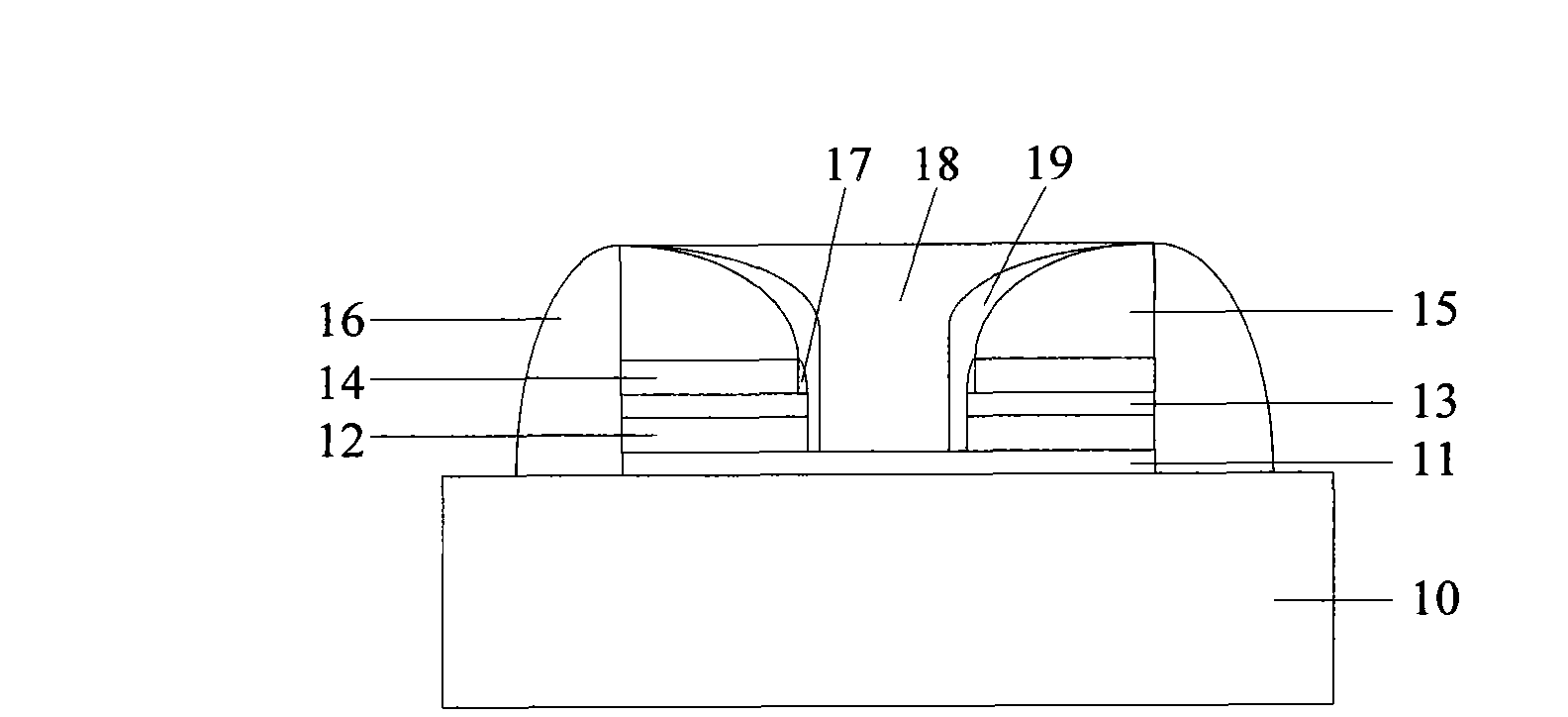
[0012] As the density of integrated circuits in existing discrete gate flash memory continues to increase, the surface area of its gate also decreases accordingly, resulting in the constant capacitance between discrete structural units in discrete gate flash memory. become smaller, affecting the performance of flash erase or write.
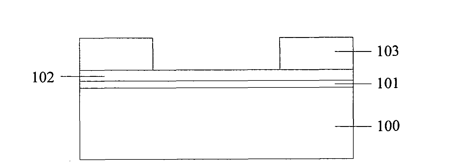
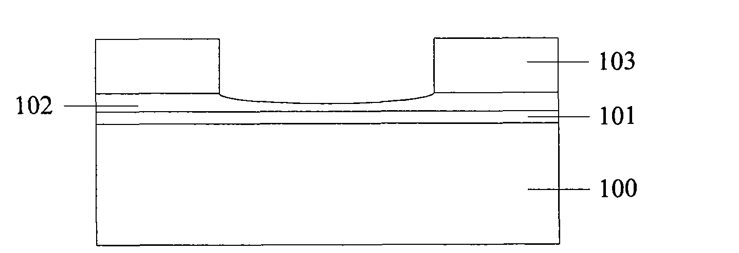
[0013] In order to solve the above-mentioned technical problem, the inventor, through a lot of experiments, found that the problem can be solved by changing the shape of the floating gate. The discrete gate flash memory obtained through the implementation of the present invention includes: a semiconductor substrate; a gate oxide layer located on the surface of the semiconductor substrate, and a discrete structural unit located on the gate oxide layer, and the discrete structural unit has: located on the gate oxide layer The floating gate, the surface of the floating gate is arc-shaped with an inclined angle; the inter-gate dielectric layer on th...
PUM
 Abstract
Description
Claims
Application Information