Semiconductor structure

A semiconductor and wide bandgap semiconductor technology, applied in semiconductor devices, electrical components, circuits, etc., can solve the problem of serious leakage of BTBT

Active Publication Date: 2010-09-01
TSINGHUA UNIV
View PDF5 Cites 30 Cited by
  • Summary
  • Abstract
  • Description
  • Claims
  • Application Information

AI Technical Summary

Problems solved by technology

[0003] The disadvantage of the existing technology is that with the continuous reduction of semiconductor size and the use of narrow bandgap semiconductor materials, BTBT leakage becomes more and more serious

Method used


Image

  • Semiconductor structure
  • Semiconductor structure
  • Semiconductor structure

Examples


Embodiment 1

[0017] In this embodiment, a wide bandgap semiconductor layer is added under the narrow bandgap semiconductor materials such as Ge, InSb, etc., so as to suppress the BTBT leakage generated at the source-drain junction when the drain terminal is highly biased. It should be noted that, in this embodiment of the present invention and the following embodiments, the so-called wide bandgap semiconductor material is only relative to Ge, InSb and other narrow bandgap semiconductor materials, such as Si, its own bandgap width is not Small, but relative to Ge, Si may be referred to as a wide bandgap semiconductor material in various embodiments of the present invention.

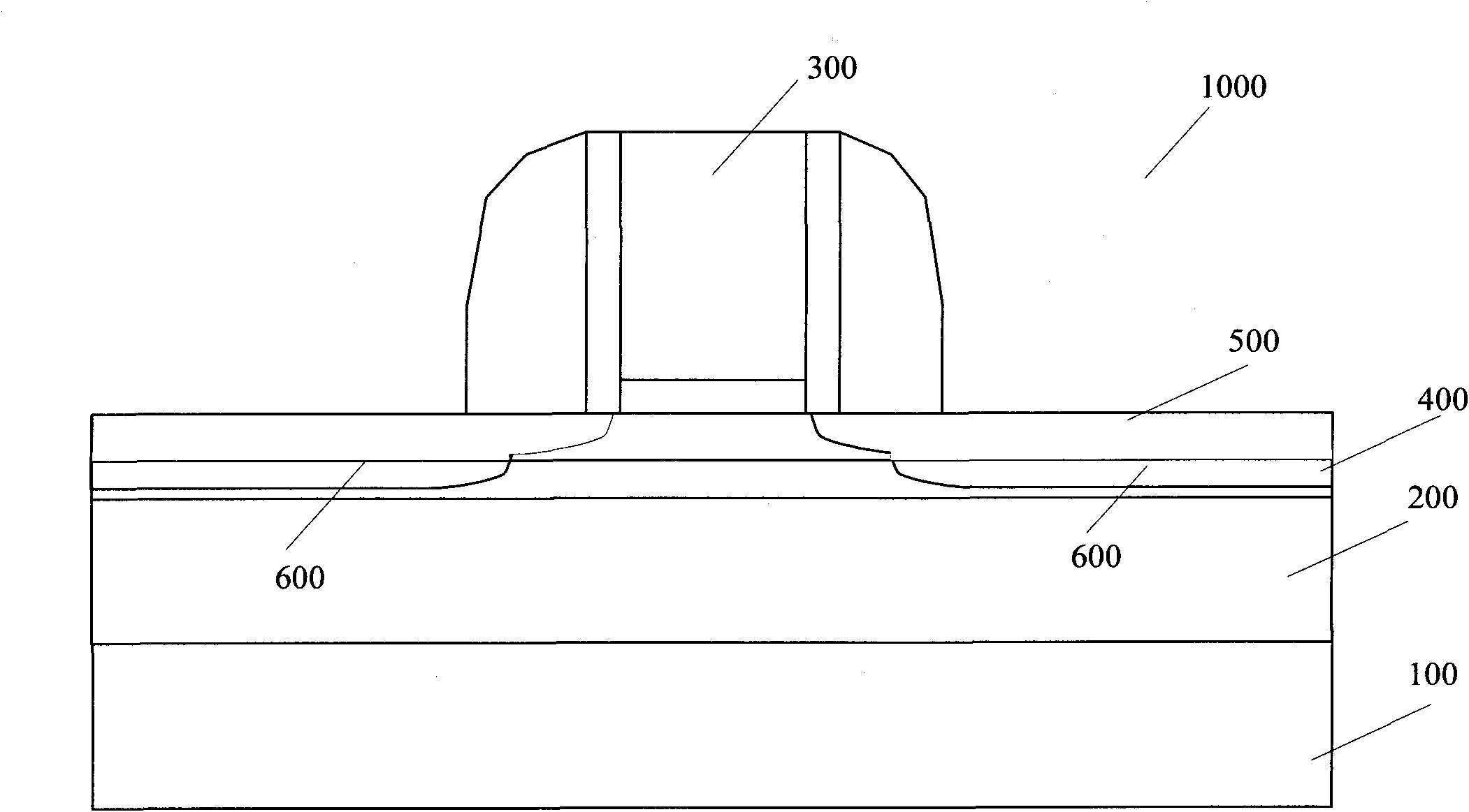
[0018] Such as figure 1 Shown is a schematic diagram of the semiconductor structure of Embodiment 1 of the present invention. The semiconductor structure 1000 may include a substrate 100, which may be any semiconductor substrate material, including but not limited to silicon, germanium, silicon germanium, SOI (silicon...

Embodiment 2

[0026] The difference from Embodiment 1 is that in this embodiment, a wide-bandgap semiconductor layer is added above the narrow-bandgap semiconductor materials such as Ge, InSb, etc., thereby suppressing GIDL leakage. Also in this embodiment, the so-called Wide bandgap semiconductor materials are only relative to narrow bandgap semiconductor materials such as Ge and InSb.

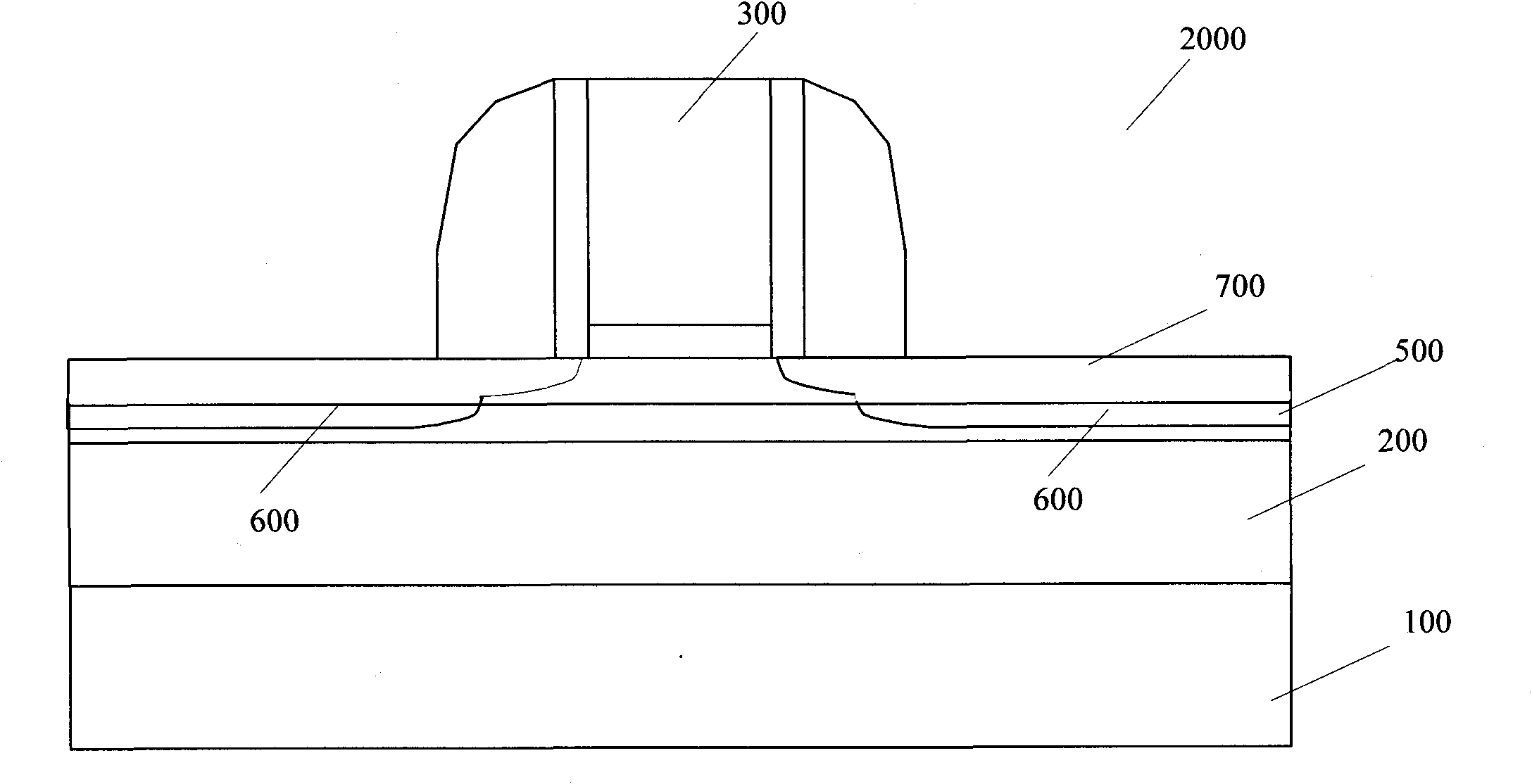
[0027] Such as figure 2Shown is a schematic diagram of the semiconductor structure of Embodiment 2 of the present invention. The semiconductor structure 2000 is similar to the semiconductor structure 1000 of the first embodiment, and also includes the substrate 100 and the transition layer or insulating layer 200 on the substrate 100, and the gate stack 300, etc., and the difference is that the semiconductor structure 2000 includes the transition layer or The strained narrow bandgap semiconductor layer 500 on the insulating layer 200 , and the second strained wide bandgap semiconductor layer 700 formed o...

Embodiment 3

[0029] In this embodiment, the advantages of the above two embodiments are combined, so that the generation of two kinds of BTBT leakage can be suppressed at the same time. In addition, this embodiment has an additional advantage that a hole potential well can be formed, thereby increasing the mobility of carriers and improving device performance.

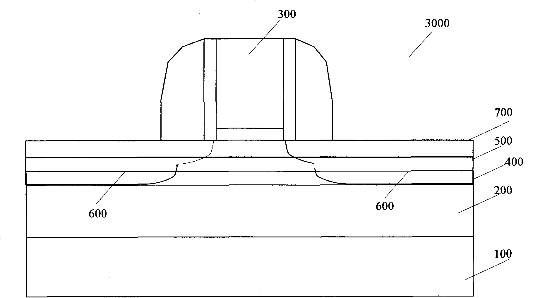
[0030] Such as image 3 Shown is a schematic diagram of the semiconductor structure of Embodiment 3 of the present invention. The semiconductor structure 3000 is similar to the above-mentioned semiconductor structures 1000 and 2000, except that in this embodiment, the above-mentioned two kinds of BTBT leakage are suppressed by using a wide bandgap semiconductor layer to surround a narrow bandgap semiconductor layer. Such as image 3 As shown, different from the above-mentioned embodiments, the semiconductor structure 3000 further includes a first strained wide bandgap semiconductor layer 400 formed on the transition layer or insu...


PUM


Abstract

The invention provides a semiconductor structure which comprises a substrate, a transition layer or an insulating layer formed on the substrate, a first strain wide bandgap semiconductor layer, a strain narrow bandgap semiconductor layer, a second strain wide bandgap semiconductor layer, a grid stacking layer formed on the second strain wide bandgap semiconductor layer, a source electrode and a drain electrode, wherein the first strain wide bandgap semiconductor layer, the strain narrow bandgap semiconductor layer and the second strain wide bandgap semiconductor layer are sequentially formed on the transition layer or the insulating layer; and the source electrode and the drain electrode are formed in the first strain wide bandgap semiconductor layer, the strain narrow bandgap semiconductor layer and the second strain wide bandgap semiconductor layer. The semiconductor structure not only can suppress the generation of two kinds of BTBT (Band-to-Band Tunneling) electric leakages, but also can generate a cavity potential well in the middle strain narrow bandgap semiconductor layer (such as a strain GE layer or a strain SiGe layer) so as to improve the mobility of carriers and the property of devices.

Description

technical field [0001] The present invention relates to the field of semiconductor manufacturing and design, in particular to a semiconductor structure, and more particularly to a semiconductor structure capable of suppressing BTBT (Band-To-Band Tunneling, Band-To-Band Tunneling) leakage of MOS devices. Background technique [0002] With the continuous improvement of semiconductor manufacturing technology, leakage current has become a very critical and non-negligible problem. Due to the narrow bandgap semiconductor material with high mobility, the bandgap width is relatively small, for example, the bandgap width of Ge is about 0.67eV, and the bandgap width of InSb is about 0.18eV, which is smaller than that of Si material. many. Therefore, with the use of high-mobility narrow-bandgap semiconductor materials such as Ge, the problem of BTBT leakage becomes more and more serious. [0003] The disadvantage of the prior art is that with the continuous reduction of semiconductor...

Claims


Application Information

Patent Timeline
Patent Type & Authority Applications(China)
IPC IPC(8): H01L29/78H01L29/06H01L29/12
CPCH01L29/7833H01L29/1054H01L29/785H01L29/7391H01L29/165
Inventor 王敬许军郭磊
Owner TSINGHUA UNIV
Why Eureka
Try Eureka