Preparation method of multiple quantum well structure for photoelectric device

A multi-quantum well structure and optoelectronic device technology, which is applied in laser components, semiconductor/solid-state device manufacturing, lasers, etc., can solve problems such as insufficient brightness, low life and low yield of semiconductor optoelectronic devices, and achieve improved recombination probability and internal Quantum efficiency, the effect of reducing energy band tilt

Active Publication Date: 2011-06-22
EPILIGHT TECH +1
View PDF1 Cites 30 Cited by
  • Summary
  • Abstract
  • Description
  • Claims
  • Application Information

AI Technical Summary

Problems solved by technology

[0005] The semiconductor optoelectronic devices produced by the ...

Method used


Image

  • Preparation method of multiple quantum well structure for photoelectric device
  • Preparation method of multiple quantum well structure for photoelectric device
  • Preparation method of multiple quantum well structure for photoelectric device

Examples


Embodiment Construction

[0024] The specific implementation steps of the present invention will be further described below in conjunction with the accompanying drawings. For the convenience of illustration, the accompanying drawings are not drawn to scale.

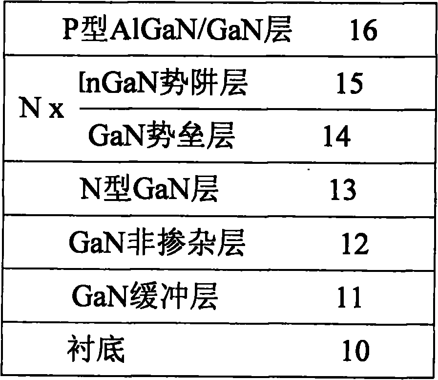
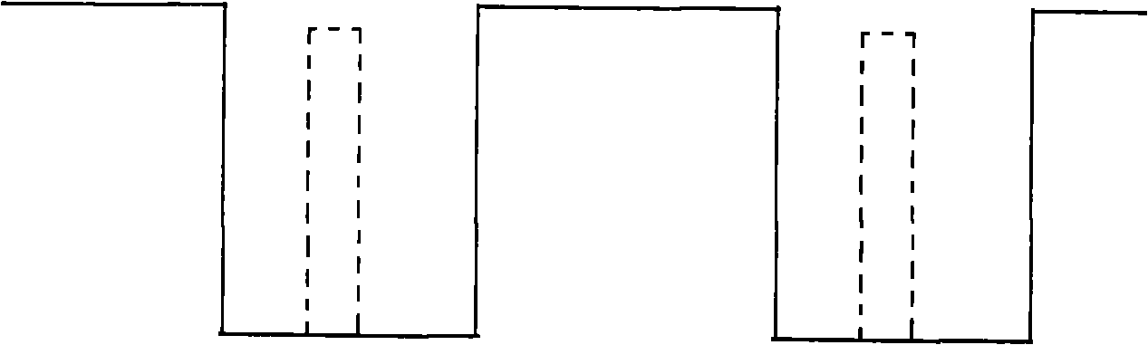
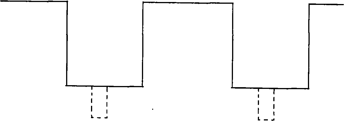
[0025] A multi-quantum well structure for a photoelectric device, the photoelectric device includes a buffer layer, a non-doped layer, an N layer, a multi-quantum well layer and a P layer, and the quantum well structure in the multi-quantum well layer includes sequentially alternating Stacked well and barrier layers. In the present invention, during the process of growing potential well layers, one layer or more than two layers of materials with energy band widths different from other potential well layers are interspersed to form insertion layers.

[0026] In the present invention, the barrier layer structure material is Al x Ga 1-x In z N, wherein 0≤xy Ga 1-y In w N, where 0≤yp Ga 1-p In q N, 0≤p<0.3, 0


PUM


Abstract

The invention discloses a preparation method of a multiple quantum well structure for a photoelectric device. The multiple quantum well structure comprises n quantum well structures which are overlapped in sequence, and each quantum well structure is formed by sequential growth of potential well layers and potential barriers, wherein the growth of each potential well layer comprises the following steps: 1, first growing an NixGa1-xN potential well layer, wherein x is more than 0.1 and less than 0.45; 2, growing a GaN insert layer; and 3, growing the InxGa1-xN potential well layer, wherein x is more than 0.1 and less than 0.45. When the potential well layer grows, one or more than two of GaN insert layers with energy band width different from that of the InxGa1-xN potential well layer and an In treatment layer grow alternately. On the one hand, the In treatment layer can stabilize the structure of the InxGa1-xN, ensures the stability of quantum well components, and controls the stability and consistency of wavelength; on the other hand, the GaN insert layer disturbs the energy band structure of a quantum well region to improve the composite rate of electron hole pairs, so that the internal quantum efficiency of device illumination is improved, and as the brightness is improved, the life test performance of the device can be improved.

Description

technical field [0001] The invention relates to a quantum well structure and a preparation method for semiconductor optoelectronic devices such as light-emitting diodes, lasers, photodetectors, solar cells, etc., in particular to a preparation method for a multi-quantum well structure for semiconductor optoelectronic devices. Background technique [0002] In recent years, the introduction of quantum well structures, especially multi-quantum well structures (MQW: Multi-Quantum-Well) has injected new vitality into the development of semiconductor optoelectronic devices, such as light-emitting diodes, lasers, and photodetectors. In the multi-quantum well structure, the potential wells in the additional periodic potential distribution along the alternate growth direction of thin layers caused by the different forbidden band widths of the two materials are called quantum wells. The forbidden band width of the potential well layer should be smaller than the forbidden band width of...

Claims


Application Information

Patent Timeline
IPC IPC(8): H01L21/205H01L33/06H01L31/18H01S5/343
CPCY02P70/50
Inventor 李淼颜建锋周健华徐黎杰郝茂盛
Owner EPILIGHT TECH
Why Eureka
Try Eureka