Tri-valued, thermal-insulating and low-power adder unit and adder

An adder, low-power technology, applied in the field of adders, can solve problems such as huge power consumption and complex circuit structure

Inactive Publication Date: 2010-09-15
NINGBO UNIV
View PDF2 Cites 10 Cited by
  • Summary
  • Abstract
  • Description
  • Claims
  • Application Information

AI Technical Summary

Problems solved by technology

However, most of the current multi-valued logic circuits are realized by using binary elements, the circuit structure is quite complicated, and the power consumption is huge.

Method used


Image

  • Tri-valued, thermal-insulating and low-power adder unit and adder
  • Tri-valued, thermal-insulating and low-power adder unit and adder
  • Tri-valued, thermal-insulating and low-power adder unit and adder

Examples


Embodiment 1

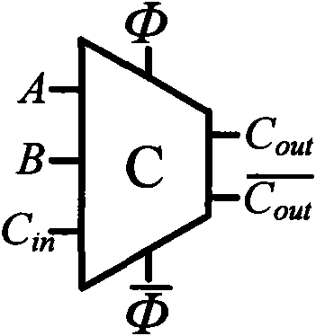
[0047] Table 1 shows the truth table of the three-value adder unit (that is, the full adder) circuit, where A and B represent the addend input signal and the augend input signal respectively, and C in Indicates the low-order carry input signal from the low-order, S and C out Respectively represent the sum output signal and the carry output signal.

[0048] Table 1 The truth table of a ternary adder unit

[0049]

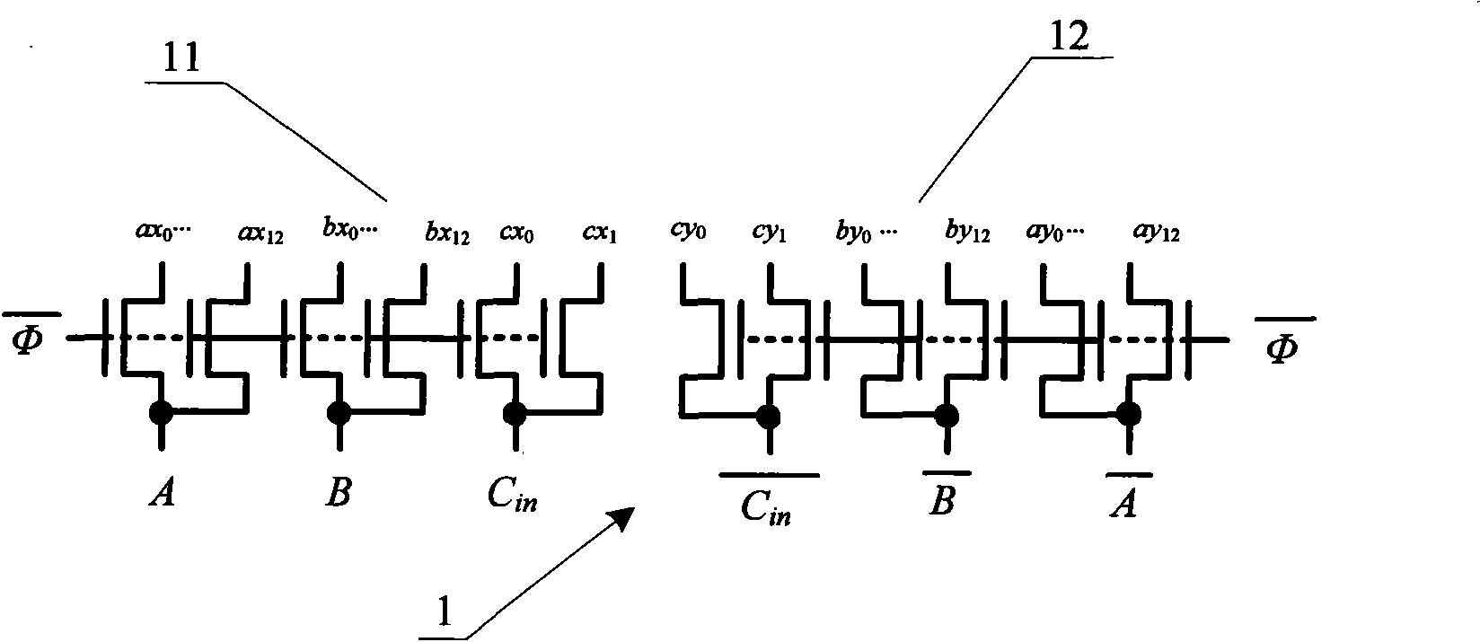
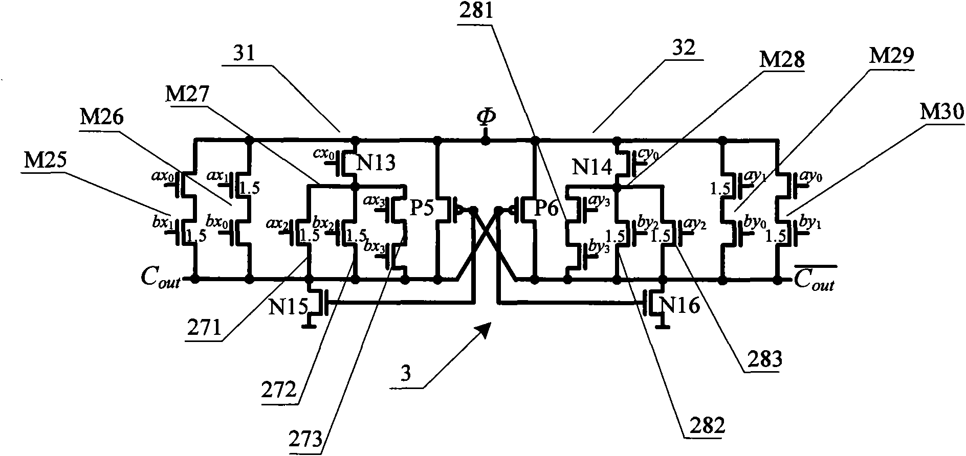
[0050] The present invention combines "Design of a DTCTGAL circuit and its application" disclosed in the Chinese Journal of Semiconductors on the basis of analyzing Table 1 (authors: Wang Pengjun, Li Kunpeng, Mei Fengna) [Journal of Semiconductors, "DTCTGAL circuit design and its application 》, Wang Pengjun, Li Kunpeng, Mei Fengna], design a ternary adiabatic low power adder unit: first use the clock signal Control the NMOS transistor to sample each input signal (including the addend input signal, the augend input signal, the low-order carry input signal, the c...

Embodiment 2

[0064] A ternary adiabatic low-power-consumption adder composed of the ternary-value adiabatic low-power-consumption adder unit given in Embodiment 1, such as Figure 9 As shown, it includes a 4-bit ternary adiabatic low-power adder unit. The first ternary-value adiabatic low-power adder unit TAFA0 is used to input the input terminal 0 of the low-order carry input signal, that is, C in =0, the first three-value adiabatic low-power adder unit TAFA0 is used to input the input terminal of the complementary low-order carry input signal to access the clocked clock signal whose amplitude level corresponds to logic 2 which is The first three-value adiabatic low-power adder unit TAFA0 is used to output the signal output terminal C of the carry output signal 0 It is connected to the signal input end of the second ternary adiabatic low-power adder unit TAFA1 for inputting the low-order carry input signal, and the first ternary adiabatic low-power adder unit TAFA0 is used to output th...


PUM


Abstract

The invention discloses a tri-valued, thermal-insulating and low-power adder unit and an adder. The adder unit controls each NMOS tube in an input signal sampling circuit to sample input signals by using a clock-controlled clock signal; four corresponding summing circuit modules and carry output circuits with cross storage-type structures are constructed by sampled values according to required realized addition logic relationship through the bootstrap operation of the NMOS tube; power clocks phi1 and phi complete the evaluation and energy recovery of the output load to realize correct logic function; and compared with a DPL tri-valued adder, the four-digit tri-valued thermal-insulating and low-power adder can save energy consumption by about 90 percent in 0.9 microsecond, and has distinct low-power characteristics.

Description

technical field [0001] The invention relates to an adder, in particular to a ternary adiabatic low power consumption adder unit and the adder. Background technique [0002] The adder unit (that is, the full adder) is the basic unit of the arithmetic circuit and one of the key components of the digital circuit system. Optimizing its design is the key to obtain a high-performance arithmetic circuit. So far, there have been various full adder design schemes, such as "45nm Low Power Consumption, High Performance Zipper CMOS Domino Full Adder Design" disclosed in the Journal of Electronics (Authors: Wang Jinhui, Gong Na, Geng Shuqin, etc.), which utilizes Charge self-compensation technology designs Zipper CMOS domino full adder to reduce power consumption by discharging dynamic nodes of P-type domino circuits to charge dynamic nodes of N-type domino circuits; Swing Complementary Pass-transistor Logic Adder" (Author: Wang Zongjing, Qi Jiayue), which uses a double differential str...

Claims


Application Information

Patent Timeline
Patent Type & Authority Applications(China)
IPC IPC(8): G06F7/50
Inventor 汪鹏君李昆鹏
Owner NINGBO UNIV
Why Eureka
Try Eureka