

Light-emitting diode packaging structure and manufacture method thereof
A technology of light-emitting diodes and packaging structures, which is applied to light sources, lighting devices, point light sources, etc., can solve the problem of uneven distribution of fluorescent materials and achieve the effect of optimal light uniformity.
- Summary
- Abstract
- Description
- Claims
- Application Information
AI Technical Summary
Problems solved by technology
Method used
Image

Examples
Embodiment Construction
[0046] In order to make the above and other objects, features and advantages of the present invention more comprehensible, the following specific embodiments are described in detail together with the accompanying drawings.
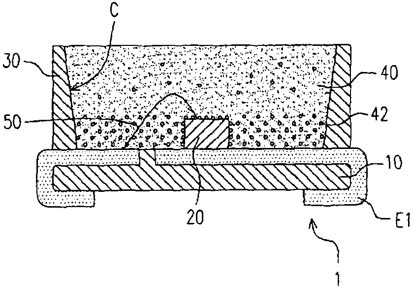
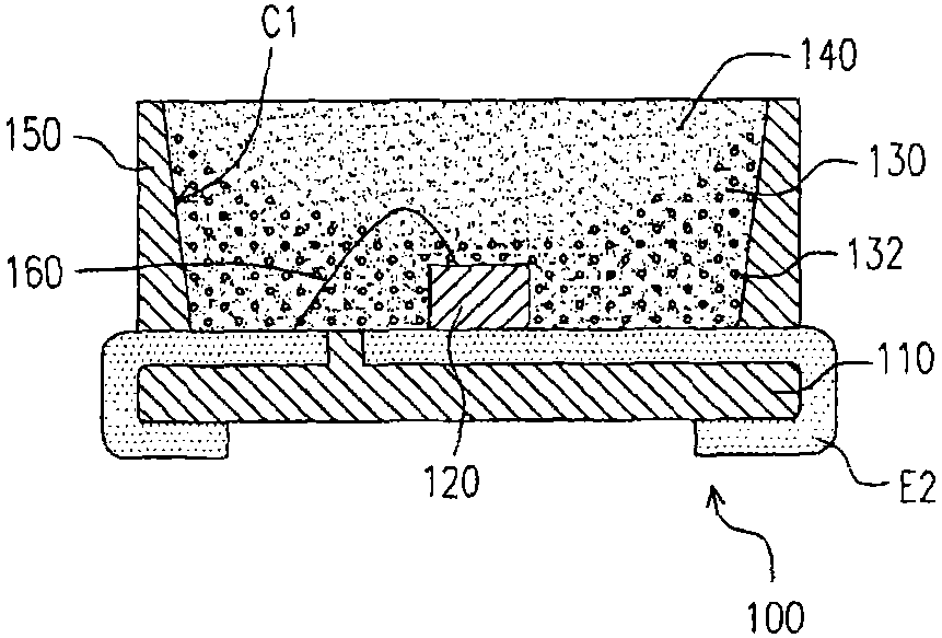
[0047] figure 2 It is a schematic cross-sectional view of a light emitting diode packaging structure according to an embodiment of the present invention. Please refer to figure 2 , in this embodiment, the LED packaging structure 100 includes a carrier 110 , a LED chip 120 , a first encapsulant 130 , a second encapsulant 140 and a housing 150 . In particular, the LED packaging structure 100 of this embodiment is a surface mount (SMD) LED packaging structure 100 .
[0048] In detail, the casing 150 is disposed on the carrier 110 and covers part of the carrier 110 , wherein the casing 150 and the carrier 110 form a cavity C1 . The light emitting diode chip 120 is disposed on the carrier 110 and accommodated in the cavity C1 to emit a light, wherein the l...
PUM
 Abstract
Description
Claims
Application Information