Manufacturing method of oriented film and LCD panel

A technology of liquid crystal display panels and manufacturing methods, applied in the direction of nonlinear optics, instruments, optics, etc., can solve problems such as lowering the qualified rate, increasing production costs, and circuit damage on the substrate, so as to avoid static electricity problems, simplify the manufacturing process, and pass rate-enhancing effect

Inactive Publication Date: 2010-09-22
INNOLUX CORP
View PDF4 Cites 11 Cited by
  • Summary
  • Abstract
  • Description
  • Claims
  • Application Information

AI Technical Summary

Problems solved by technology

[0005] Since the known technology uses a contact method to form the alignment film, that is, rubbing the alignment film to form dents, powder debris will remain in the process, requiring washing equipment to wash, thus increasing the manufacturing process steps and costs
In addition, other unexpected dents or scratches may occur during friction, which will reduce the yield, and the electrostatic problem caused by friction may also easily cause damage to the circuit on the substrate.
In addition, orientation equipment can also increase production costs

Method used


Image

  • Manufacturing method of oriented film and LCD panel
  • Manufacturing method of oriented film and LCD panel
  • Manufacturing method of oriented film and LCD panel

Examples


Embodiment Construction

[0023] A method for manufacturing an alignment film for a liquid crystal display panel and a method for manufacturing a liquid crystal display panel according to a preferred embodiment of the present invention will be described below with reference to related drawings, wherein the same components will be described with the same symbols.

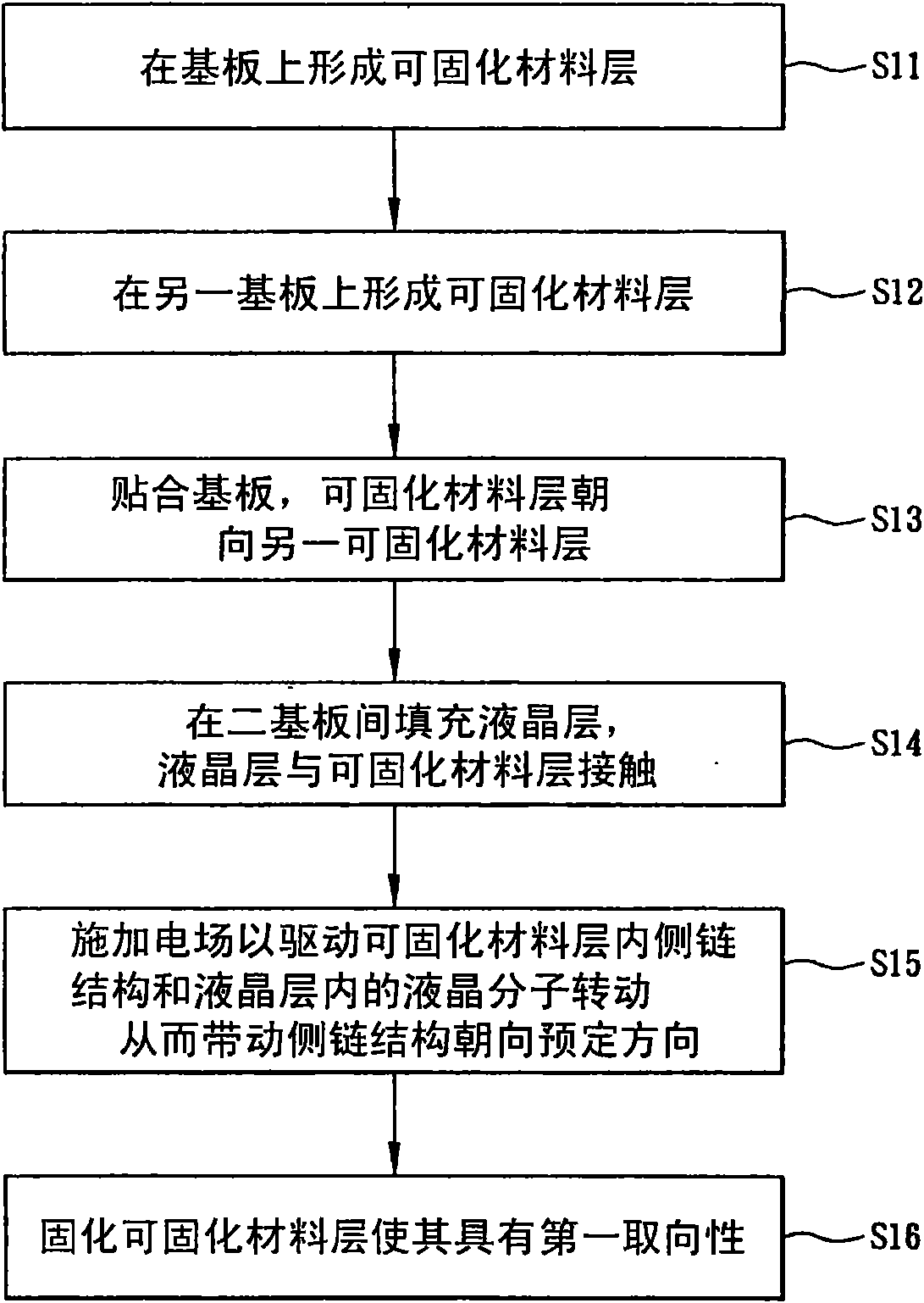
[0024] figure 2 It is a flow chart of a method for manufacturing a liquid crystal display panel in a preferred embodiment of the present invention. In this embodiment, the manufacturing method mainly includes step S11 to step S16. The following fit Figure 3A to Figure 3D The manufacturing method of this example will be described.

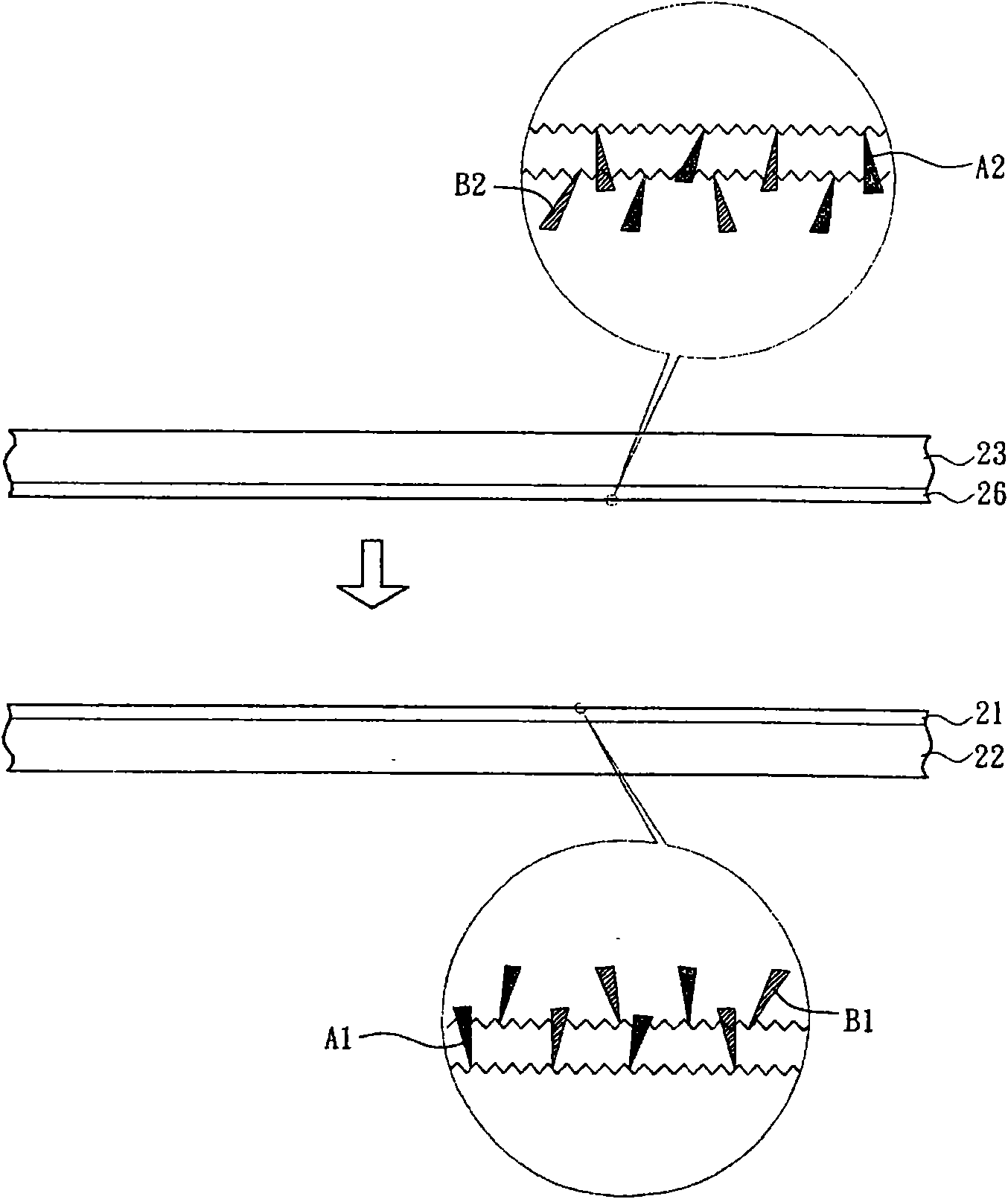
[0025] Such as figure 2 and Figure 3A As shown, step S11 is to form a curable material layer 21 on the substrate 22, wherein the curable material has a side chain structure A1. Step S12 is to form another curable material layer 26 on another substrate 23 , wherein the other curable material has another sid...


PUM


Abstract

The invention discloses a manufacturing method of an oriented film, comprising: forming a solidifiable material layer with a side chain on a first substrate; sticking a first substrate and a second substrate to cause the solidifiable material layer to face the second substrate; filling a liquid crystal layer between the first substrate and the second substrate to ensure that the liquid crystal layer can be contacted with the solidifiable material layer; applying an electric field to cause the side chain to face a preset direction; solidifying the solidifiable material layer to cause the side chain to be in crosslinking and be solidified, and ensuring that the solidifiable material layer has liquid crystal orientation. The manufacturing method of an LCD panel comprises: forming a first UV-curing material layer with a first side chain on the first substrate; forming a second UV-curing material layer with a second side chain on the second substrate; sticking the first substrate and the second substrate to cause the first UV-curing material layer to face the second UV-curing material layer; filling the liquid crystal layer between the first substrate and the second substrate; causing the liquid crystal layer to contact with the first UV-curing material layer and the second UV-curing material layer; applying a first electric field to cause the first side chain to face the first preset direction; and photocuring the first UV-curing material layer to cause the UV-curing material layer to have the first orientation.

Description

technical field [0001] The present invention relates to a method for manufacturing an alignment film, and in particular to a method for manufacturing an alignment film for a liquid crystal display panel. Background technique [0002] Liquid crystal display (Liquid Crystal Display, LCD) has gradually replaced traditional cathode ray tube (Cathode Ray Tube, CRT) display device due to its advantages such as light and thin body, low power consumption and no radiation, and is applied to various electronic products. For liquid crystal display devices, how to simplify the manufacturing process and save the manufacturing cost has always been an urgent need to be solved. [0003] Generally speaking, the manufacturing process of a liquid crystal display device mainly includes an array manufacturing process (Array Process), a panel manufacturing process (Cell Process) and a module manufacturing process (Module Process). Among them, the array manufacturing process is mainly to form ele...

Claims


Application Information

Patent Timeline
Patent Type & Authority Applications(China)
IPC IPC(8): G02F1/1337G02F1/1333
Inventor 李汉郎庄正旭
Owner INNOLUX CORP
Why Eureka
Try Eureka