Broken-line etching design method of soft printed circuit board electroplating lead

A technology for printed circuit boards and electroplating leads, applied in printed circuits, printed circuit manufacturing, electrical components, etc., can solve problems such as metal wire residues and hidden dangers of short circuits, and achieve the effect of eliminating hidden dangers of short circuits

Active Publication Date: 2010-09-22
CHUNHUA TECHNOLOGICAL KUSN
View PDF2 Cites 4 Cited by
  • Summary
  • Abstract
  • Description
  • Claims
  • Application Information

AI Technical Summary

Problems solved by technology

The disadvantages of this method are: ①When the circuit board is double-sided or multi-layered, the holes cannot be punched because the lines on other layers cannot get out of the way; The customer's organization is assembled with metal, which may cause short circuit hazards

Method used


Image

  • Broken-line etching design method of soft printed circuit board electroplating lead
  • Broken-line etching design method of soft printed circuit board electroplating lead
  • Broken-line etching design method of soft printed circuit board electroplating lead

Examples


Embodiment Construction

[0019] The present invention will be further described below in conjunction with the embodiment shown in accompanying drawing:

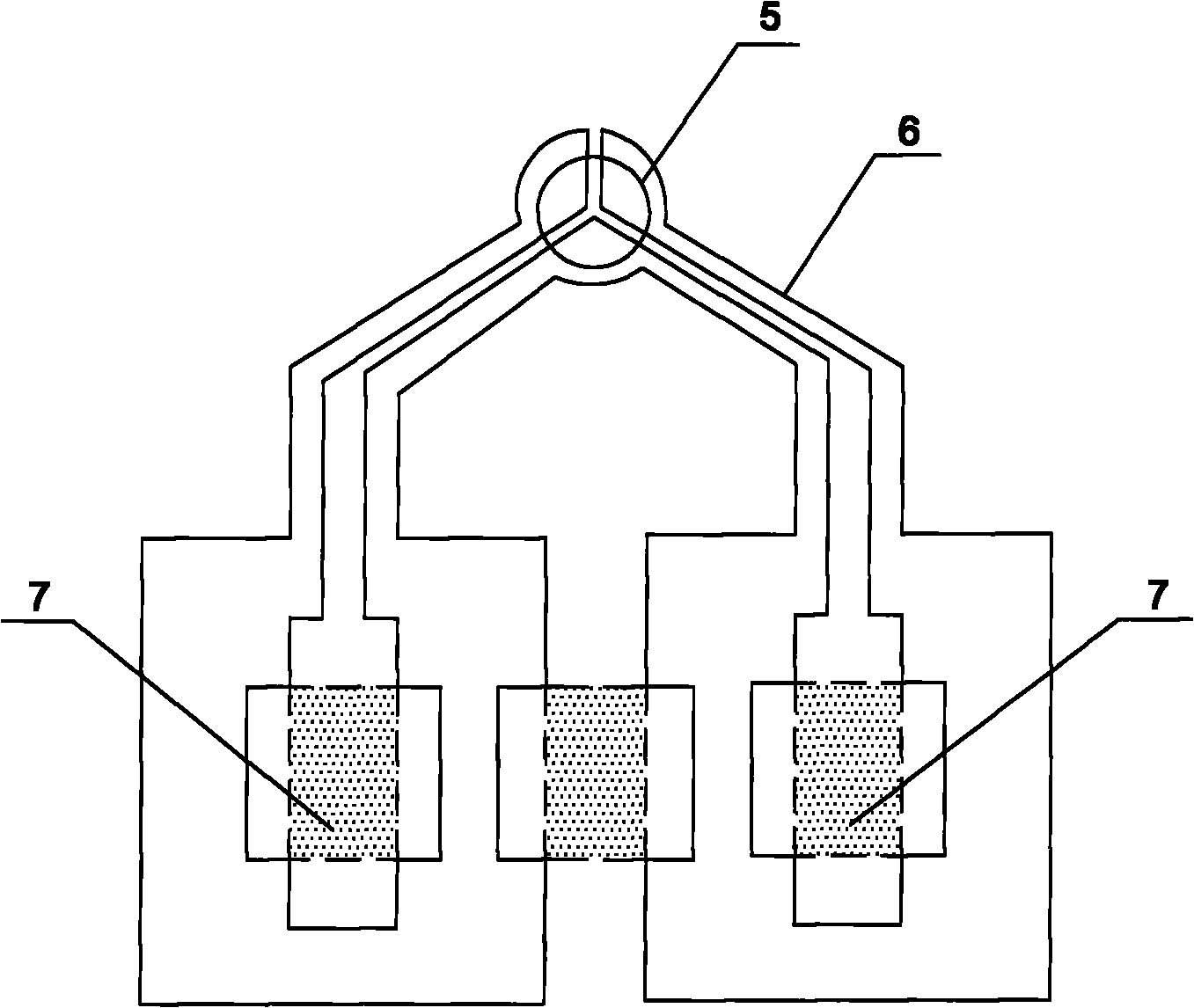
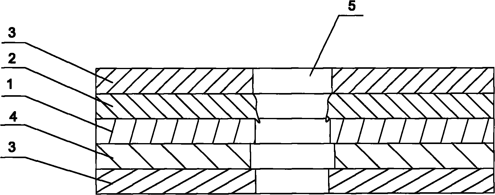
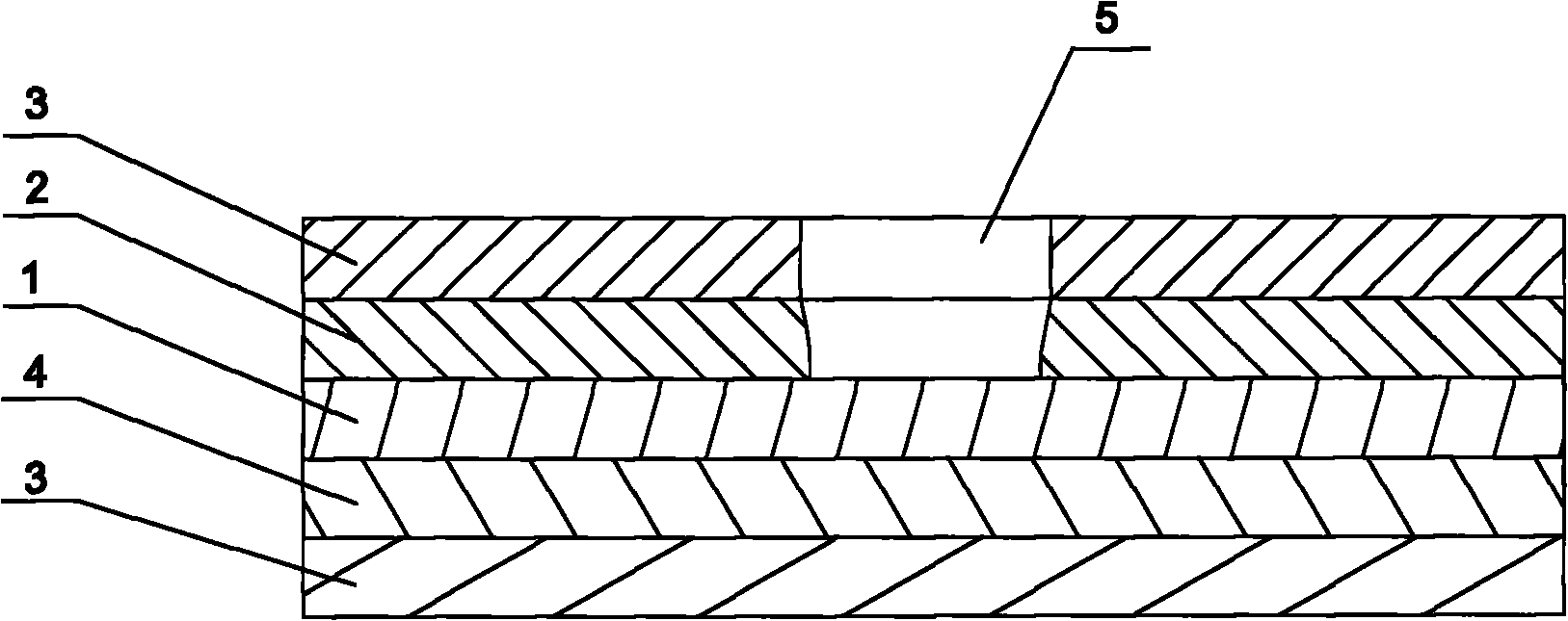
[0020] See attached figure 1 And attached figure 2 . The circuit board includes a substrate 1 including a first surface and a second surface, a circuit layer 2 covering the first surface of the substrate 1, a solder resist layer 3 covering the circuit layer 2, and a circuit layer covering the substrate 1. The back circuit layer 4 on the second surface, and the solder resist layer 3 covering the back circuit layer 4 . During electroplating, the electroplating leads 6 are drawn out from the circuit layer 2 to deposit nickel and gold on the surface of the electroplating plate 7. After electroplating, the electroplating leads 6 need to be disconnected.

[0021] When using the original method to disconnect the electroplating lead 6, punch a hole at the position of the disconnection hole 5, the position of the back circuit layer 4 corresponding to the ...


PUM


Abstract

The invention provides a broken-line etching design method of a soft printed circuit board electroplating lead, comprising the following steps: (1) previously opening a broken-line hole on a solder mask layer, keeping the position of the broken-line hole corresponding to the position of the electroplating lead which requires to be broken on a circuit layer so as to expose the electroplating lead which requires to be broken out of the broken-line hole; (2) fully covering the broken-line hole with a film made of a plating-proof medium, and performing electroplating treatment on the position of a circuit board in need of electroplating; (3) removing the film made of the plating-proof medium at the position of the broken-line holes after electroplating treatment so as to expose the electroplating lead out of the broken-line hole; (4) covering the part of the circuit board besides the broken-line hole by the film made of the plating-proof medium so as to expose the electroplating lead out of the broken-line hole; and (5) removing the electroplating lead exposed in the broken-line hole by an etching method so as to disconnect the electroplating lead. For the circuit board made by the method, cabling on other layers is not affected by the broken-line hole, and short-circuit hidden trouble does not occur.

Description

technical field [0001] The invention relates to a method for manufacturing a flexible printed circuit board. Background technique [0002] Gold electroplating of flexible printed circuit board refers to the electrolytic reaction in the solution with the help of external direct current, so that nickel gold is deposited on the surface of the exposed part of the copper foil of the flexible board. This method requires that the electroplating part must be led out by electroplating leads. must be disconnected. The currently used method of disconnecting the electroplating lead is: punching holes in a mold to interrupt the electroplating lead at the position of the electroplating lead. The disadvantages of this method are: ①When the circuit board is double-sided or multi-layered, the holes cannot be punched because the lines on other layers cannot get out of the way; The client mechanism is assembled with metal which presents a short circuit hazard. Contents of the invention ...

Claims


Application Information

Patent Timeline
Patent Type & Authority Applications(China)
IPC IPC(8): H05K3/00H05K3/18
Inventor 莫卫龚
Owner CHUNHUA TECHNOLOGICAL KUSN
Why Eureka
Try Eureka