

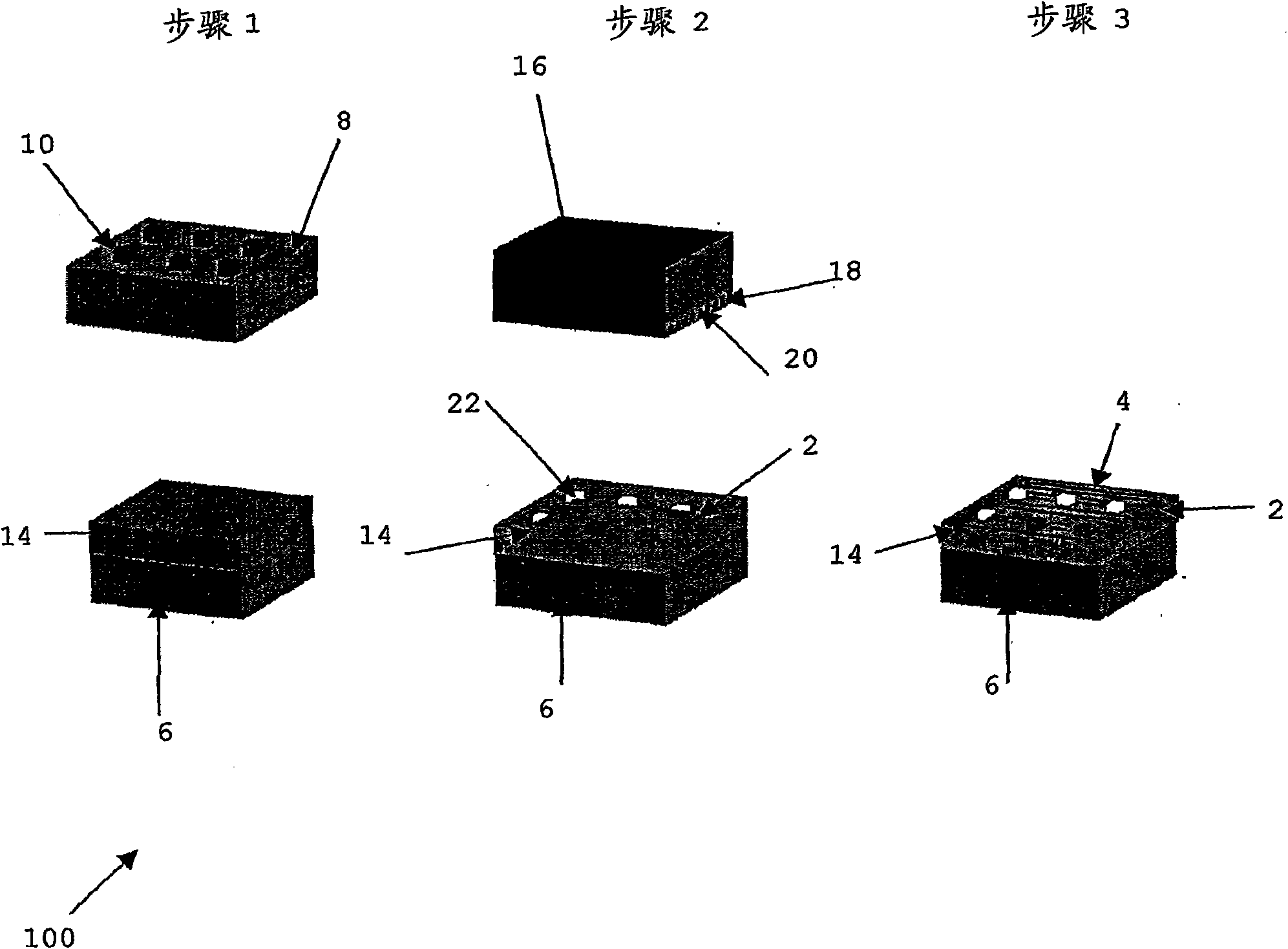
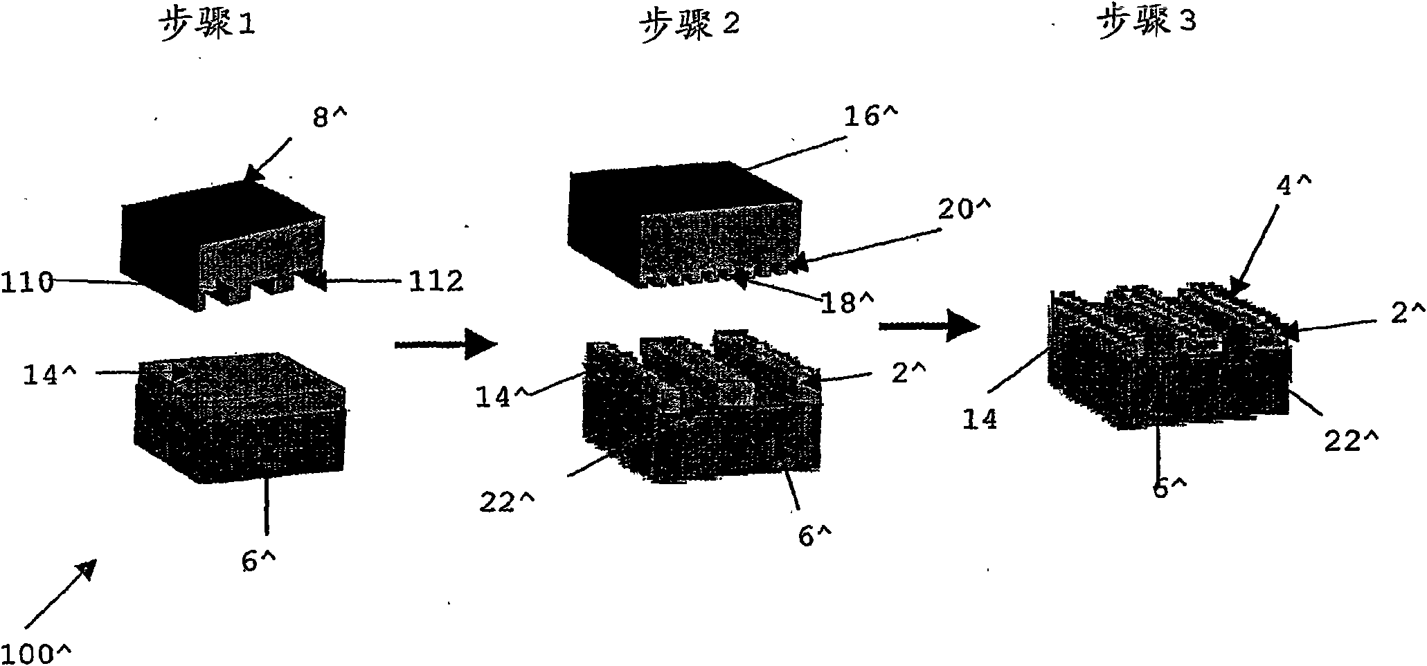
A method of manufacturing an organic electronic or optoelectronic device
A technology for organic electronic devices and optoelectronic devices, applied in the direction of electric solid devices, electrical components, semiconductor devices, etc., can solve the problems of increasing manufacturing time and cost, organic solution spread, device degradation, etc.
- Summary
- Abstract
- Description
- Claims
- Application Information
AI Technical Summary
Problems solved by technology
Method used
Image

Examples
Embodiment approach 1
[0154] In this example for SU-8 TM 2000 The contact angles of water and anisole on glue materials are discussed.
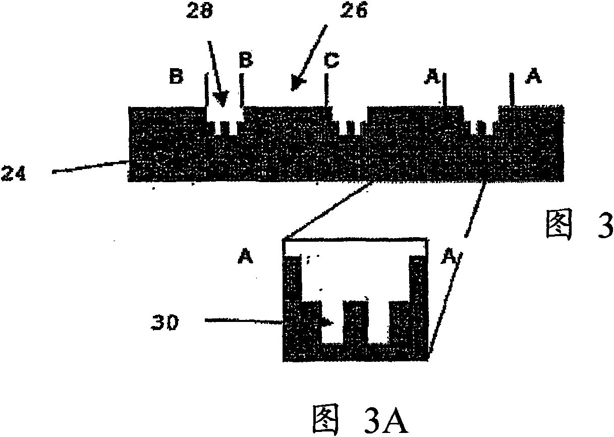
[0155] As mentioned above, the SU-8 TM Glue 2000 was used as the polymeric material to form the banks to direct the flow of the organic solution into the respective wells. Contains SU-8 TM The banks of the 2000 glue were embossed with an embossed formation having a grid and grooves with a width and height of 2 microns. Table 1 shows the contact angles (θx, θy) of water and anisole and the change in contact angle (Δθ).
[0156] Table 1: Contact angle measurements for water and anisole
[0157]
[0158] The term "post-cure" refers to the SU-8 TM 2000 Glue Results Status. SU-8 TM Glue 2000 is first exposed to UV light to start the crosslinking process and then heated to complete the crosslinking. SU-8 in this state TM 2000 glue is called "post-cure".
[0159] As can be seen from Table 1, when water is placed on the imprint formations with a width an...
PUM
 Abstract
Description
Claims
Application Information