
Semiconductor integrated circuit compensating jitter and jitter compensation method

A data transmission and circuit technology, applied in electrical components, digital memory information, static memory, etc., can solve problems such as uneven clock cycle, wrong output data, wrong input data gating operation, etc.

Inactive Publication Date: 2010-10-13
SAMSUNG ELECTRONICS CO LTD
View PDF3 Cites 14 Cited by
  • Summary
  • Abstract
  • Description
  • Claims
  • Application Information

AI Technical Summary

Problems solved by technology

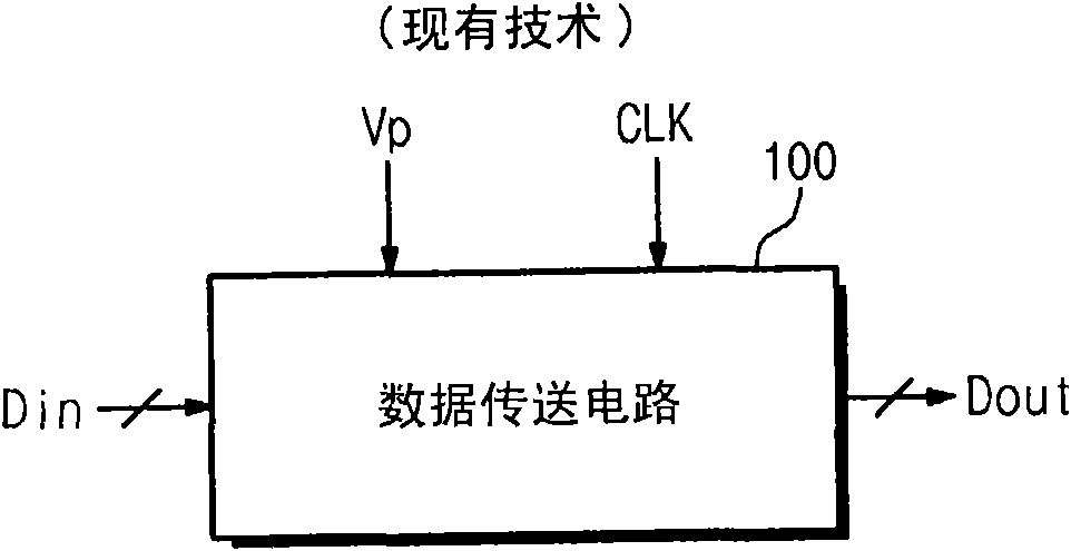
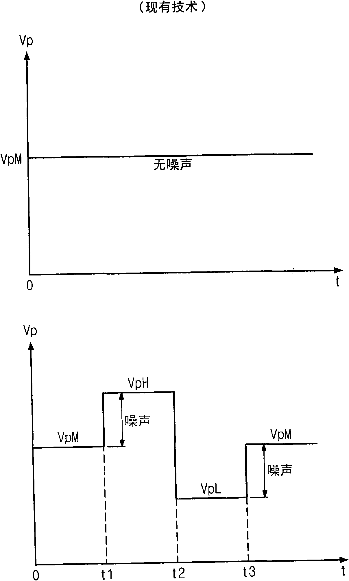
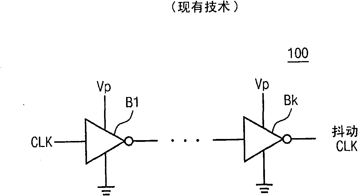
However, the wrong clock edge and uneven clock period of the jittered clock signal lead to multiple erroneous input data (Din) gating operations and output data (Dout) to provide wrong data content

Method used


Image

  • Semiconductor integrated circuit compensating jitter and jitter compensation method
  • Semiconductor integrated circuit compensating jitter and jitter compensation method
  • Semiconductor integrated circuit compensating jitter and jitter compensation method

Examples


Embodiment Construction

[0041] Reference will now be made to specific embodiments of the inventive concepts illustrated in the accompanying drawings. Throughout the drawings and written description, the same reference numbers and labels are used to refer to the same or similar elements, signals and features.

[0042] It should be noted that the inventive concept can be embodied in many different ways. Accordingly, the inventive concept should not be construed as limited to the illustrated embodiments. Rather, these embodiments are presented as illustrative examples only.

[0043] Those skilled in the art will appreciate that recitation terms (eg, first, second, etc.) are only used to distinguish different elements. These terms should not define a certain numerical limitation for such elements.

[0044] As used herein, the term "and / or" includes any and all combinations of one or more of the associated listed items. It will also be understood that when an element is referred to as being "connected...


PUM


Abstract

The invention relates to a semiconductor integrated circuit compensating jitter and a jitter compensation method. A data I / O interface for an integrated circuit device includes a noise detector receiving a power supply voltage, detecting a power supply voltage noise component, and providing a clock delay control signal in response to detected power supply voltage noise component. The data I / O interface also includes a clock delay circuit providing a delayed clock signal in response to the clock delay control signal, and a data transfer circuit powered by the power supply voltage and providing output data synchronously with the delayed clock signal.

Description

[0001] Cross References to Related Applications [0002] This US nonprovisional patent application claims priority to the Korean patent application filed on April 8, 2009 under 35 U.S.C § 119, the subject matter of which is incorporated herein by reference. technical field [0003] The inventive concept relates generally to data transfer circuits, integrated circuit devices incorporating data transfer circuits, and methods of controlling the operation of data transfer circuits that compensate for clock signal jitter that occurs in accordance with power supply voltage variations. compensate. Background technique [0004] As integrated circuit devices are increasingly required for greater data bandwidth and increased functionality, the transmission frequency at which data is received by and transmitted from such devices has increased. Increasing the data input / output (I / O) frequency causes many problems because conventional circuits are generally not adapted to operate at suc...

Claims


Application Information

Patent Timeline
IPC IPC(8): G11C16/06
CPCH03K5/1565H03K2005/0013G11C7/22
Inventor 裴升浚朴光一金荣植郭相协
Owner SAMSUNG ELECTRONICS CO LTD
Learn More