Supercharge Your Innovation With Domain-Expert AI Agents!

Patterning method and integrated circuit structure

A patterning and patterning technology, applied in circuits, electrical components, electrical solid-state devices, etc., can solve problems such as large costs, and achieve the effect of saving costs and enhancing competitiveness.

Active Publication Date: 2010-10-13
MACRONIX INT CO LTD
View PDF0 Cites 12 Cited by
  • Summary
  • Abstract
  • Description
  • Claims
  • Application Information

AI Technical Summary

Problems solved by technology

As a result, the factory may have to pay a considerable cost to replace the matching new machines

Method used


Image

  • Patterning method and integrated circuit structure
  • Patterning method and integrated circuit structure
  • Patterning method and integrated circuit structure

Examples


Embodiment Construction

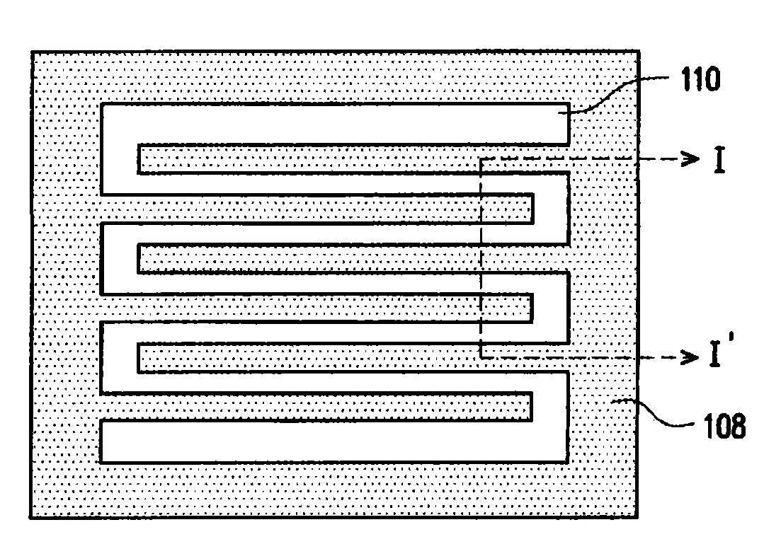
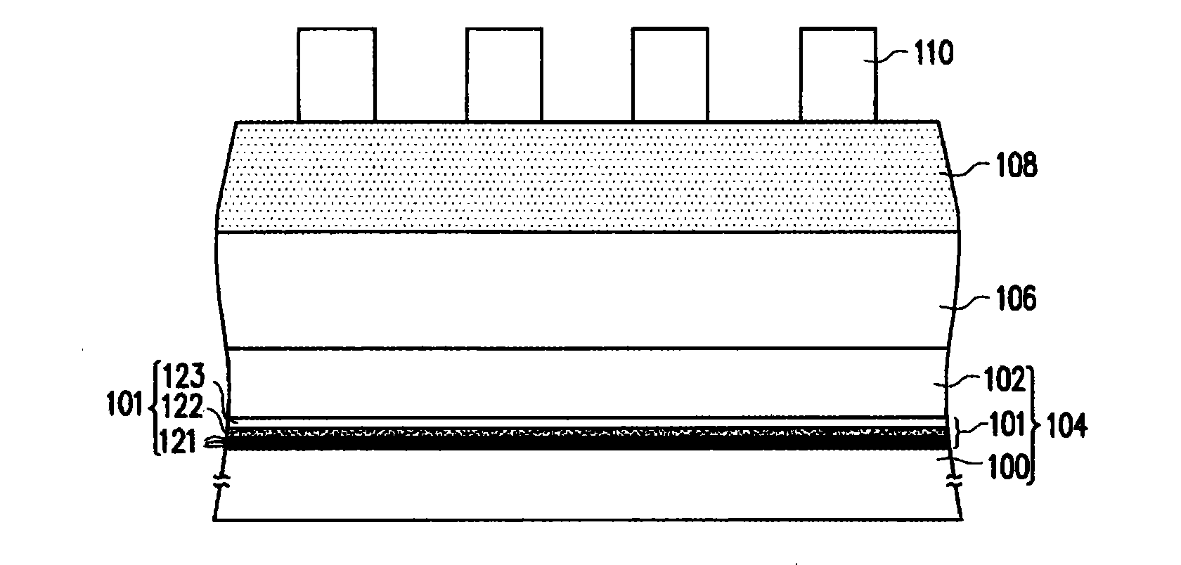
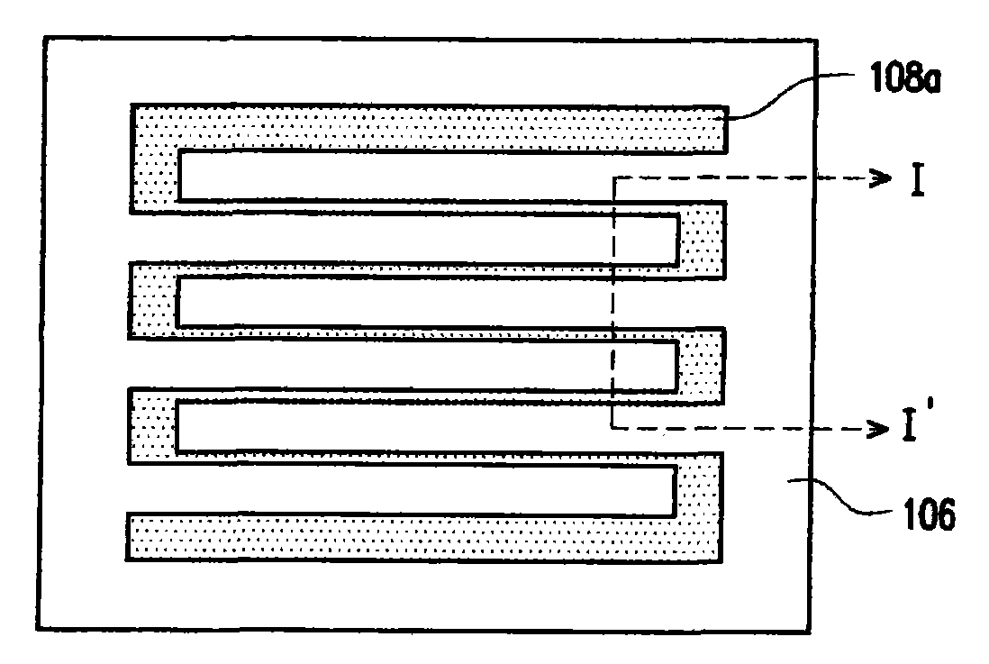
[0036] Figures 1A to 1I It is a top view of the flow of the patterning method according to an embodiment of the present invention. Figures 2A to 2I is based on Figures 1A to 1I Process section diagram drawn along line I-I'.

[0037] First, please refer to Figure 1A and 2A , sequentially forming a mask layer 106 , a transfer layer 108 and a patterned photoresist layer 110 on the target layer 104 . The target layer 104 is, for example, a laminated structure, including a dielectric layer 101 and a material layer 102 sequentially formed on the substrate 100 . The substrate 100 is, for example, a semiconductor structure such as a silicon substrate. The dielectric layer 101 can be a single-layer or multi-layer structure. The material of the material layer 102 is, for example, polysilicon or metal. The material of the mask layer 106 includes silicon dioxide formed by tetraethoxysiloxane (TEOS-SiO 2 ), borophosphosilicate glass (BPSG), phosphosilicate glass (PSG), hydrogenat...


PUM


Abstract

A patterning method is provided. First, a mask layer and a plurality of first transfer patterns are sequentially formed on a target layer. Thereafter, a plurality of second patterns is formed in the gaps between the first transfer patterns. Afterwards, a plurality of third transfer patterns is formed, wherein each of the third transfer patterns is in a gap between a first transfer pattern and a second transfer pattern adjacent to the first transfer pattern. A portion of the mask layer is then removed, using the first transfer patterns, the second transfer patterns and third transfer patterns as a mask, so as to form a patterned mask layer. Further, a portion of the target layer is removed using the patterned mask layer as a mask.

Description

technical field [0001] The invention relates to a patterning method and an integrated circuit structure. Background technique [0002] Non-volatile memory has the advantages of being able to store, read, and erase data multiple times, and the stored data will not disappear after power off. Therefore, non-volatile memory is widely used in personal Computers and electronic equipment and more. [0003] As the integration level of the non-volatile memory increases day by day, the size of the non-volatile memory must also be reduced accordingly. The miniaturization and integration of components is an inevitable trend, and it is also an important topic for active development in all walks of life, and the key technology is the photolithography process. [0004] In the photolithography process, it is known that manufacturing line width or line spacing below 65 nanometers, especially the line width / line spacing (line / space) does not exceed 25 / 25 nanometers, which is quite difficult...

Claims


Application Information

Patent Timeline
Patent Type & Authority Applications(China)
IPC IPC(8): H01L21/033H01L21/8247H01L27/115H10B69/00
CPCH01L21/32139H01L27/11521H01L21/0337H01L27/11517H01L27/115H01L21/0338H01L27/11568H10B41/00H10B69/00H10B41/30H10B43/30
Inventor 吕函庭
Owner MACRONIX INT CO LTD
Features
  • R&D
  • Intellectual Property
  • Life Sciences
  • Materials
  • Tech Scout
  • Unparalleled Data Quality
  • Higher Quality Content
  • 60% Fewer Hallucinations
Learn More