OLED monitor and packaging method thereof

An encapsulation method and display technology, which can be applied to instruments, identification devices, etc., can solve the problems of increasing the distance between the substrate 1 and the back cover 2, increasing the thickness of the display, and increasing the weight of the display, so as to achieve the effect of reducing the weight and reducing the thickness.

Inactive Publication Date: 2010-10-20
TRULY SEMICON
View PDF5 Cites 22 Cited by
  • Summary
  • Abstract
  • Description
  • Claims
  • Application Information

AI Technical Summary

Problems solved by technology

However, the use of the desiccant 6 increases the weight of the display and also increases the distance between the substrate 1 and the back cover 2, that is, increases the thickness of the display, so that the advantages of light and thin OLED displays cannot be realized.

Method used


Image

  • OLED monitor and packaging method thereof
  • OLED monitor and packaging method thereof
  • OLED monitor and packaging method thereof

Examples


Embodiment 1

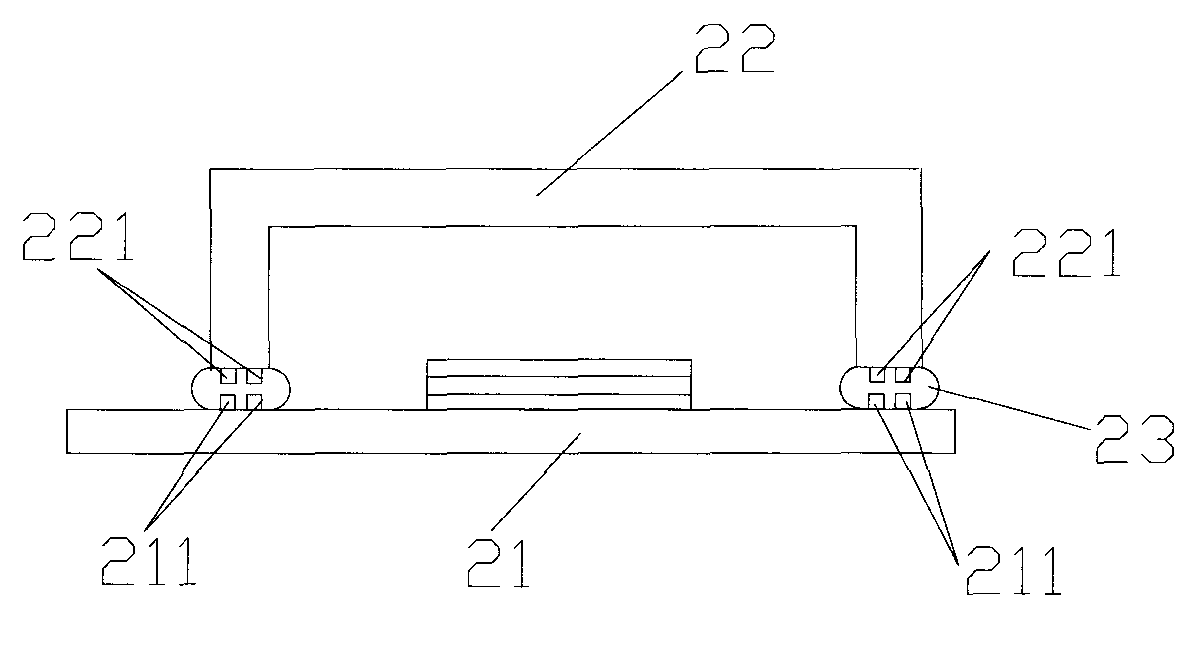
[0040] Such as figure 2 Shown is a cross-sectional view of the OLED display in this embodiment. The display includes a substrate 21 and a back cover 22 that are bonded to each other. The substrate 21 in the bonding area has a first protrusion 211 facing the back cover 22, and the back cover 22 has The second protrusions 221 facing the substrate 21, the first protrusions 211 and the second protrusions 221 correspond to each other, and are wrapped in the packaging glue 23.

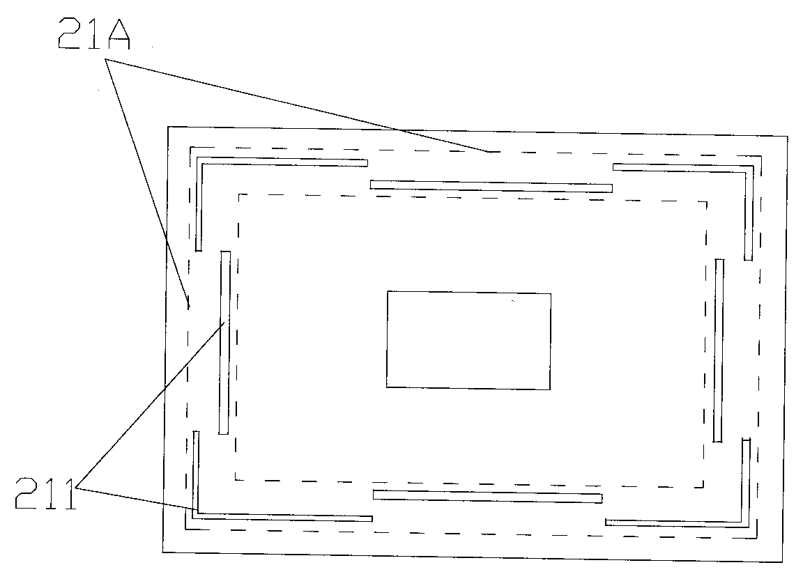
[0041] Such as image 3 Shown in this embodiment is the top view of the display substrate 21. In the center is the stacked cathode, organic functional layer and anode. Near the edge of the substrate 21 is the annular bonding area 21A of the substrate 21 and the back cover 22. It has a square ring shape. In this area, two incomplete first protrusions 211 are arranged along the square ring. The first protrusions 211 on the outer ring are arranged at the four corners of the square ring, and the first protrusions 2...

Embodiment 2

[0045] Such as Figure 4 Shown is a cross-sectional view of the OLED display in the second embodiment. The display includes a substrate 41 and a back cover 42 that are bonded to each other. The substrate 41 in the bonding area has a first protrusion 411 facing the back cover 42, and the back cover 42 There are second protrusions 421 facing the substrate 41, and the first protrusions 411 and the second protrusions 421 are distributed alternately and are wrapped in the packaging glue 43.

[0046] Such as Figure 5 Shown is a top view of the display substrate 41 in this embodiment. Located in the center is the stacked cathode, organic functional layer and anode. Near the edge of the substrate 41 is the annular bonding area 41A between the substrate 41 and the back cover 42. The ring is a square ring, of course, it can also be a circular ring. It has a ring shape, and two complete first protrusions 411 are arranged along a square ring in this area. Of course, the two first protrusion...

Embodiment 3

[0050] Such as Figure 7 Shown is a cross-sectional view of the OLED display in the third embodiment. The display includes a substrate 71 and a back cover 72 that are bonded to each other. The substrate 71 in the bonding area has a first protrusion 711 facing the back cover 72, and the back cover 72 There are second protrusions 721 facing the substrate 71, and the first protrusions 711 and the second protrusions 721 are alternately distributed with each other and are wrapped in the packaging glue 73.

[0051] The mechanism of the substrate in this embodiment is similar to that in the second embodiment, and will not be repeated here.

[0052] Such as Picture 8 Shown is a top view of the back cover 72 of the display in this embodiment. Near the edge of the back cover 72 is the annular bonding area 72A of the substrate 71 and the back cover 72, the bonding area 72A corresponds to the bonding area on the substrate 71, and three complete second circles are arranged in the bonding area ...


PUM


Abstract

The invention provides an OLED monitor and a packaging method thereof. The OLED monitor comprises a substrate and a rear cover which are mutually jointed; the substrate and the rear cover are provided with circular jointed areas; the substrate is provided with a first lug which is arranged in the jointed area along a circular shape and towards the rear cover, and the rear cover is provided with a second lug which is arranged in the jointed area along the circular shape and towards the substrate; the first lug and the second lug are mutually staggered or correspond to each other; and the jointed areas of the substrate and the rear cover are sealed through sealant. The lugs, which are arranged on the substrate and the rear cover, are staggered or correspond to each other, can effectively shade the vapor, oxygen and the like outside the monitor, greatly reduce the vapor, oxygen and the like which invade into the monitor so as to protect the monitor without drier, reduce the impact of vapor and the like to the service life and the like of the monitor, reduce the weight of the monitor and reduce the thickness of the monitor.

Description

Technical field [0001] The present invention relates to the technical field of displays, in particular to an OLED display and a packaging method thereof. Background technique [0002] Organic Light-Emitting Diode (OLED) displays, also known as organic electroluminescent displays, are a new type of flat panel display. Compared with LCD, OLED has many advantages: ultra-light, ultra-thin, high brightness, large viewing angle, pixel self-luminescence, low power consumption, fast response, etc. Therefore, OLED has been generally regarded by the industry as the most promising new generation display technology. [0003] The structure of the existing OLED is as figure 1 As shown, it includes: a substrate 1 and a back cover 2, wherein an anode 3, an organic functional layer 4 covering the anode 3, and a cathode 5 on the organic functional layer 4 are deposited on the substrate 1, and the back cover 2 faces the cathode 5 A desiccant 6 is attached to one side of the, in order to ensure the ...

Claims


Application Information

Patent Timeline
Patent Type & Authority Applications(China)
IPC IPC(8): G09F9/33
Inventor 曹绪文张雪峰何基强
Owner TRULY SEMICON
Why Eureka
Try Eureka