Storage device, computer system, and storage device access method

a storage device and access method technology, applied in the field of storage devices, computer systems, and storage device access methods, can solve the problems that address conversion is required to be performed with a unit, and achieve the effect of preventing intensive rewriting, facilitating rapid and flexible access to the address table, and effective techniqu

Active Publication Date: 2007-05-31
SONY CORP
View PDF3 Cites 92 Cited by
  • Summary
  • Abstract
  • Description
  • Claims
  • Application Information

AI Technical Summary

Benefits of technology

[0080] The invention has advantages of being able to apply an effective technique using address conversion to manage user data as it is to operate an address table on a flash memory. This advantageously implements swift and flexible access making to the address table, prevents intensive rewriting to any one specific erase block, and simplifies the management and operation of the address table.

Problems solved by technology

The problem here is that if effective management is aimed, it means that the address conversion is required to be performed with a unit smaller in size.

Method used


Image

  • Storage device, computer system, and storage device access method
  • Storage device, computer system, and storage device access method
  • Storage device, computer system, and storage device access method

Examples


first embodiment

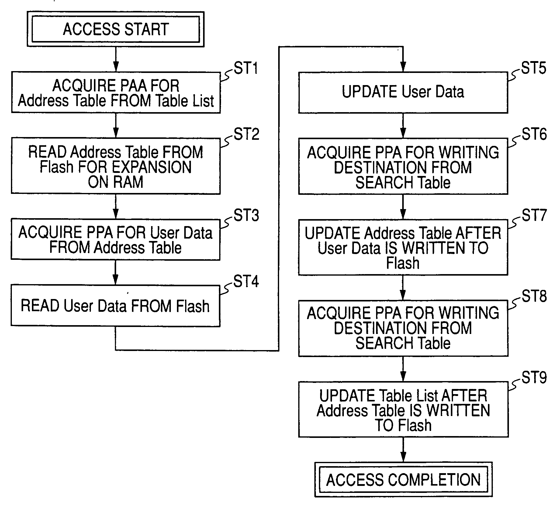
[0106]FIG. 5 is a diagram showing an exemplary configuration of a computer system in which a storage device of the invention is adopted.

[0107] A computer system COMSYS is configured to include, mainly, a file storage device 30, and a host system (processing device) 50.

[0108] The file storage device 30 is configured to include an interface circuit (I / F) 31, a control circuit 32, an internal bus 33, a page buffer 34, NAND flash memories 35 and 36, a control circuit 37, and a memory bus 38.

[0109] The control circuit 32 includes a RAM (Random Access Memory) 40, which carries therein a table list 41, an address table 42, and a search table 43.

[0110] The host system 50 is configured to include a CPU (Central Processing Unit), a RAM, a ROM (Read Only Memory), a system bus, and others.

[0111] In the file storage device 30, the 32-bit memory bus 38 is connected in parallel with the two-chip 8 Gb NAND flash memories (also referred to as flash memory chips) 35 and 36 having an input / output ...

second embodiment

[0188] Described next is the invention, caching of an address table.

[0189] If the flash memory is accessed every time the user data is accessed and the address table is operated as in the first embodiment, a no-negligible overhead is generated by data access even if the access operation is executed at high speed. Therefore, it is considered desirable to reserve an area of the RAM 40 as a cache memory of the address table, and reduce the frequency of access making directly to the flash memory module 39.

[0190] To update any cached address table, write-back caching leads to better efficiency compared with write-through caching. With the write-back caching, the update result is collectively reflected to the flash memory at the time of entry release, for example, and with the write-through caching, the update result is reflected to the flash memory whenever the data is updated.

[0191] For such caching, desirably, instead of a single entry, a plurality of address tables may be stored as ...

third embodiment

[0226] In the third embodiment, entries of any cached table are managed in the format corresponding to the table index (T-Index) of a table list 41b. That is, tag fields of the entries in a cache table 45b each carry therein a table index (T-Index).

[0227] Described below is the procedure of accessing user data in the third embodiment with a correlation to the access flowchart of FIG. 12.

[0228] Steps ST21 and ST22:

[0229] When a sector address of “0x05502C” comes from the host system 50 together with an access command for user data, a table index “0x050” is generated from the high-order address thereof, and the value thereof is used to search the cache table 45b, thereby checking whether there is any cache hit or not.

[0230] The cache table 45b has eight entries, each corresponding to a predetermined storage area inside of the RAM 40A. The entries are managed by round-robin scheduling (first-in first-out), and any new entry is added to the last. The head entry and the tail entry are...


PUM


Abstract

A storage device that includes: an address table; a cache memory; a flash memory device being a storage medium for user data; and a control circuit that is in charge of access management for the flash memory device. In the storage device, the control circuit makes access to the user data on the flash memory device via an address table, in the address table, with an index of an address value generated from an initial logical address, location information is acquired for the user data on the flash memory device corresponding to the index, and the address table is segmented in its entirety into a plurality of small address tables for every area of the index, and the small address tables being segmentation results are stored in the flash memory device, read as required when the user data is accessed, and expanded on the cache memory with entries of the small address tables.

Description

CROSS REFERENCES TO RELATED APPLICATIONS [0001] The present invention contains subject matter related to Japanese Patent Applications JP2005-346660, JP2006-135058 and JP 2006-245687 filed in the Japanese Patent Office on Nov. 30, 2005, May 15, 2006 and Sep. 11, 2006, respectively, the entire contents of which being incorporated herein by reference. BACKGROUND OF THE INVENTION [0002] 1. Field of the Invention [0003] The present invention relates to a storage device including a nonvolatile memory, and a computer system and, more specifically, to a storage device whose main storage medium is a flash memory, a computer system, and a storage device access method. [0004] 2. Description of the Related Art [0005] In recent years, flash memories are receiving attention as a storage medium for use for digital still cameras or mobile computer equipment. [0006] The flash memory is a semiconductor memory for storing therein data. For data storage, using electron tunneling or acceleration of hot ...

Claims


Application Information

Patent Timeline
Patent Type & Authority Applications(United States)
IPC IPC(8): G06F12/08
CPCG06F12/0246G06F12/0292G06F12/1027G11C16/08G11C16/10
Inventor NISHIHARA, TOSHIYUKI
Owner SONY CORP
Why Eureka
Try Eureka