

Semiconductor memory apparatus and refresh control method of the same
A memory and semiconductor technology, applied in static memory, digital memory information, information storage, etc., can solve the problems of data volatility, difficult to use semiconductor memory device storage units, etc.
- Summary
- Abstract
- Description
- Claims
- Application Information
AI Technical Summary
Problems solved by technology
Method used
Image

Examples
Embodiment Construction
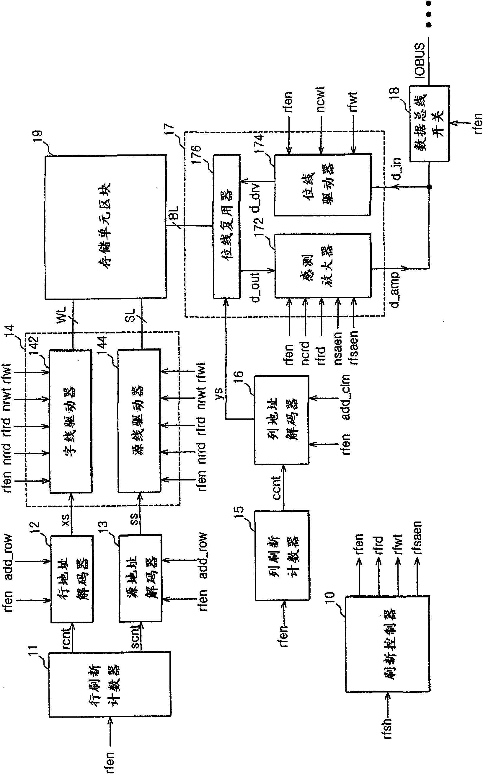
[0030] figure 2 is a block diagram showing the configuration of a memory core area of a semiconductor memory device according to one embodiment.
[0031] Such as figure 2 As shown, the semiconductor memory device may include a refresh controller 10, a row refresh counter 11, a row address decoder 12, a source address decoder 13, a row operation controller 14, a column refresh counter 15, a column address decoder 16, a column operation control device 17, data bus switch 18 and memory cell block 19.
[0032] The refresh controller 10 may generate a refresh enable signal rfen, a refresh read signal rfrd, a refresh write signal rfwt, and a refresh sense amplification enable signal rfsaen in response to the refresh signal rfsh. The row refresh counter 11 may generate a multi-bit row count signal rcnt and a multi-bit source count signal scnt by performing a count operation in response to the refresh enable signal rfen. The row address decoder 12 may generate the multi-bit row...
PUM
 Abstract
Description
Claims
Application Information