Clock synchronous circuit

A clock synchronization and circuit technology, applied in the field of data transmission, can solve the problems of short delay unit delay time, large balanced delay, and data cannot be accurately collected, and achieve the effect of making up for the lack of balance

Active Publication Date: 2010-10-20
BRITE SEMICON SHANGHAI CORP
View PDF3 Cites 10 Cited by
  • Summary
  • Abstract
  • Description
  • Claims
  • Application Information

AI Technical Summary

Problems solved by technology

However, the delay time of the delay unit of CML is very short (such as 30ps), and the delay time that needs to be balanced is large (such as 300ps), so a large number of delay units are required
Moreover, the clocks of all CML circuits have to add the same delay, which greatly increases the power consumption of the system (each delay unit current 200uA)
In addition, when the external environment changes, the delay of the CML level to CMOS Logical level conversion circuit will also change. The method of increasing the delay on the CML clock, because it adopts an open-loop structure without feedback loop, It is uncontrollable, so when the level conversion delay that requires balance changes beyond a certain range, the delay unit delay of CML cannot meet the balance requirements, resulting in data that cannot be accurately collected

Method used


Image

  • Clock synchronous circuit
  • Clock synchronous circuit
  • Clock synchronous circuit

Examples


Embodiment Construction

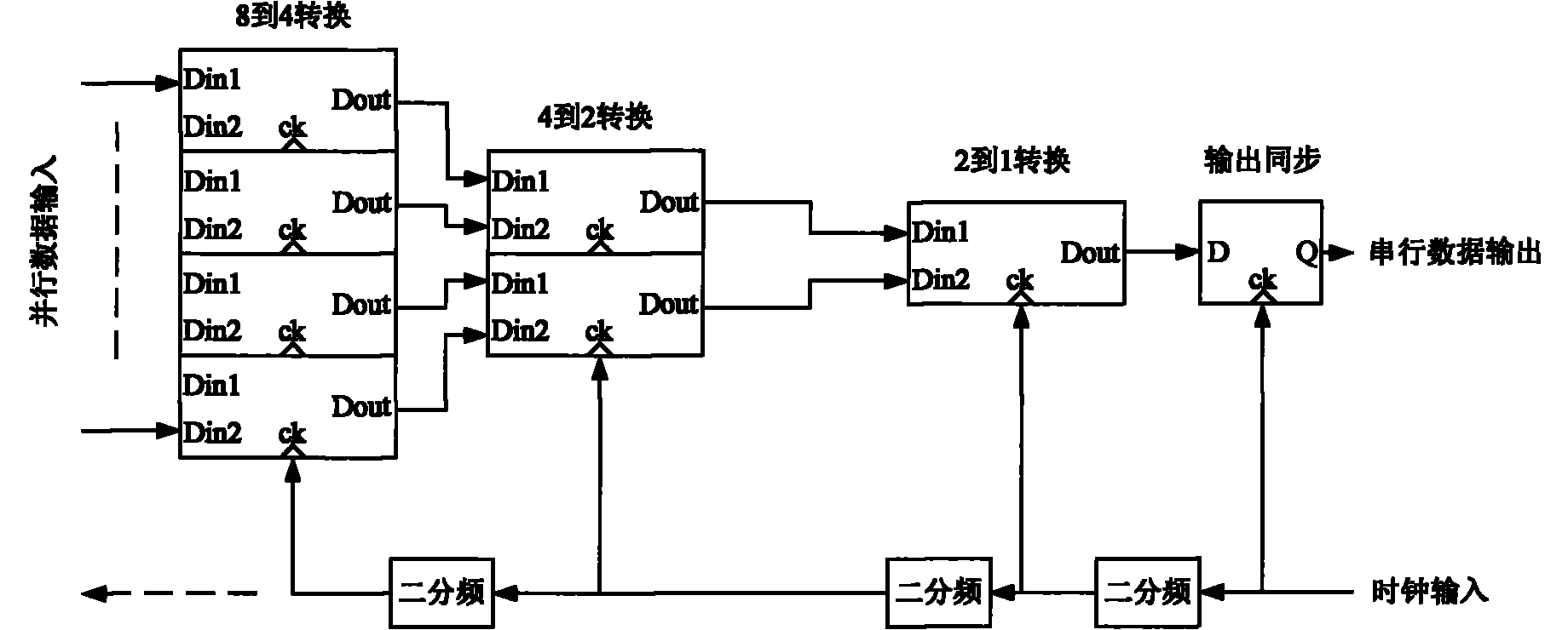
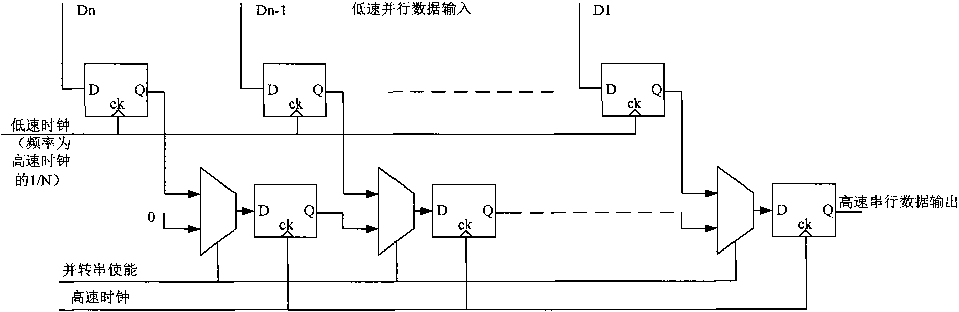
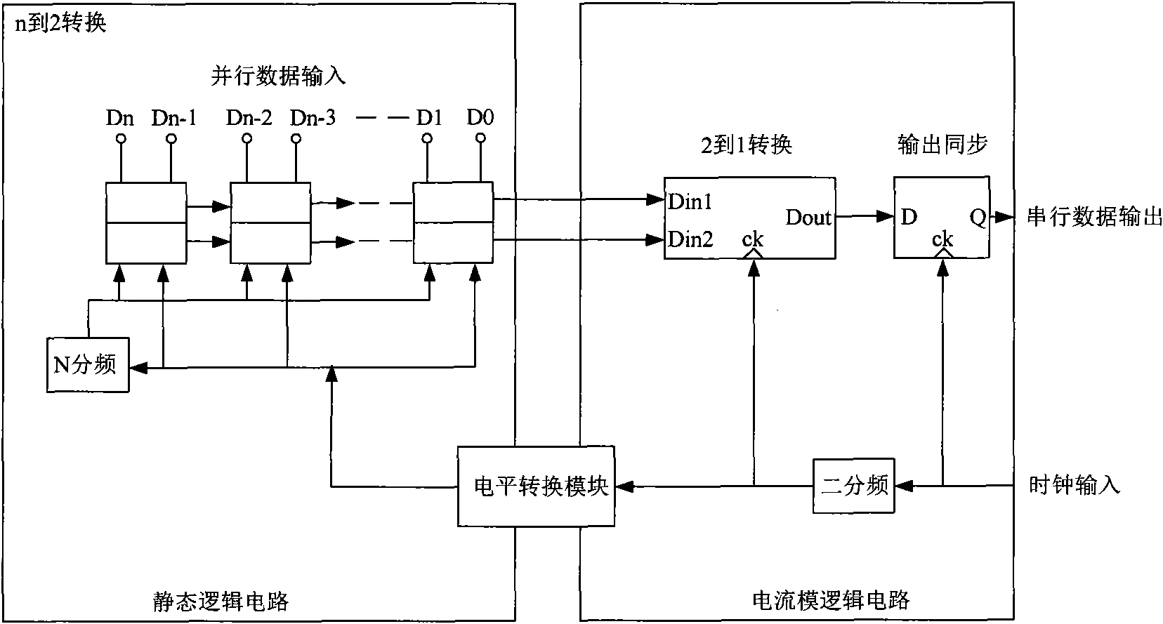
[0029] Figure 4 It is a schematic structural diagram of a parallel-to-serial conversion circuit with a delay chain loop, which can explain the application of the present invention. The delay chain loop of the present invention can achieve synchronization before and after the clock signal level conversion, and the reliability is enhanced and more economical than the prior art. power consumption. Figure 4 The parallel-serial conversion circuit shown includes static logic circuit (parallel-serial conversion circuit with shift register structure), current mode logic circuit (parallel-serial conversion circuit with tree structure) and delay chain loop. The delay chain circuit includes a delay chain module, two level conversion modules, a sampling module, and a delay chain control module. The clock signal used by the current mode logic circuit is a CML level clock signal. The clock signal is converted into a CMOS Logical level clock after being level-converted and then adopted by...


PUM


Abstract

The invention discloses a clock synchronous circuit applied in a high-speed parallel data serialization system, which comprises a delay chain module, a delay chain control module, a sampling module and a level conversion module. The modules form a controllable delay chain circuit in a high-speed parallel data serialization system with the combination of a tree-structure parallel and serial conversion circuit and a shifting register parallel and serial conversion circuit, and the synchronization of two different level clocks is achieved via the delay on CMOS Logical clock level. Compared with the prior art, the delay is controllable, and the power consumption of the system is greatly saved.

Description

technical field [0001] The invention relates to the field of data transmission, more specifically, to a clock synchronization circuit in high-speed parallel data serialization. Background technique [0002] At present, there are mainly two high-speed parallel data serialization technologies: tree structure (Tree Architecture) and shift register structure (Shift-Register Architecture). The unit circuit of the tree structure is a two-to-one parallel-to-serial conversion circuit (MUX2: 1). As the number of parallel data bits increases, the required MUX2: 1 unit increases exponentially, which makes the parallel-serial conversion using only the tree structure Circuits become bulky, leading to excessively large and costly components. However, due to the structure of the shift register itself, its working speed will not be very high, which makes the parallel-to-serial conversion circuit using only the shift register structure slower. And because the bit width of the parallel inpu...

Claims


Application Information

Patent Timeline
Patent Type & Authority Applications(China)
IPC IPC(8): H03M9/00H03K5/135
Inventor 卞兴中庄志青黄明
Owner BRITE SEMICON SHANGHAI CORP
Why Eureka
Try Eureka