Semiconductor laser aging clamp

A technology of lasers and semiconductors, applied in the direction of semiconductor lasers, lasers, laser components, etc., can solve problems such as difficulty in probe alignment, small electrode area, damage to lasers, etc., to achieve power management and communication, simple fixture design , the effect of reducing the difficulty of alignment

Inactive Publication Date: 2010-10-27
INST OF SEMICONDUCTORS - CHINESE ACAD OF SCI
View PDF3 Cites 15 Cited by
  • Summary
  • Abstract
  • Description
  • Claims
  • Application Information

AI Technical Summary

Problems solved by technology

This method has the following disadvantages: First, the method of probe contact needs to accurately place the probe on the laser or lead out to the electrode on the substrate. In terms of physical size, the length and width of the semiconductor laser core are generally 300 Micron, the electrode area is very small, and it is difficult to align the probe; secondly, because the contact direction is perpendicular to the electrode surface, it is very likely that the electrode will be broken or even damaged during the alignment and pressing process.
Due to the above-mentioned shortcomings, the method of using metal probes for aging puts a lot of pressure on the positioning fixture. The fixture mechanism used in this method requires high precision and stability, which brings great pressure to mechanical design and processing. Great pressure came, introduced a considerable cost

Method used


Image

  • Semiconductor laser aging clamp
  • Semiconductor laser aging clamp

Examples


Embodiment Construction

[0021] The present invention adopts a new idea of ​​replacing vertical contact with surface contact. Aiming at the two limitations of the traditional method: vertical contact and small contact area, the new method adopted by the present invention mainly includes the following aspects.

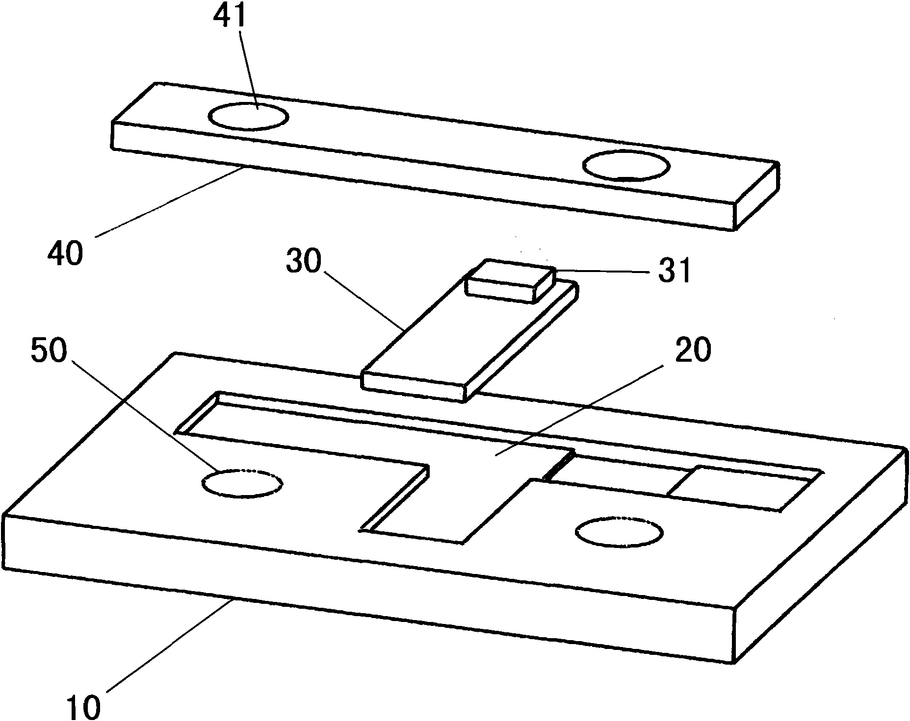
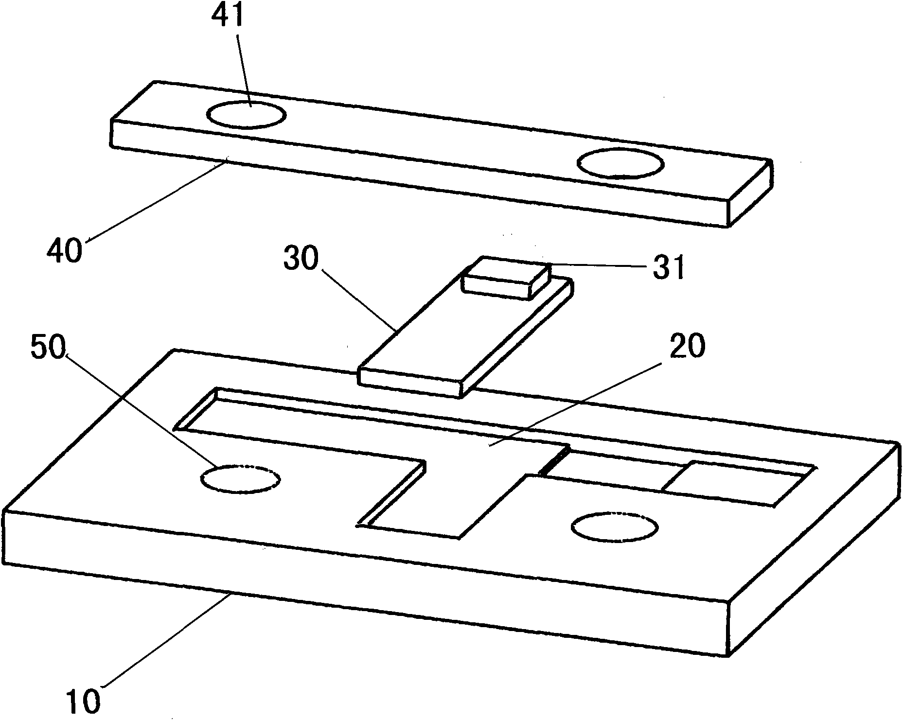
[0022] see figure 1 As shown, the present invention provides an aging fixture suitable for semiconductor lasers, which includes: a main body 10, which can adopt a three-layer printed circuit board, and the thickness of the surface layer is equal to the depth of the groove 20. The depth of the groove 20 should be designed according to the thickness of the heat sink 30 used, so that the heat sink 30 can be submerged in the groove 20 without being blocked by the groove 20 from the optical path of the laser 31 on the heat sink 30 . Therefore, the electrode sinking process can be used to form a groove 20 structure with a required depth, and limit the spatial position of the heat sink 30 while ensur...


PUM


Abstract

The invention provides a semiconductor laser aging clamp which comprises a main body, a heat sink and a cover plate, wherein the main body is a printed circuit board, a square, bar-shaped or T-shaped groove is arranged in the middle of the main body, and screw holes are arranged at two sides of the groove on the main body and correspond to circular holes on the cover plate; the heat sink with a laser is positioned in the groove; and the cover plate is used for covering the heat sink, and the circular holes are arranged at two sides on the upper surface of the cover plate and used for fixing the cover plate on the main body through screws.

Description

technical field [0001] The invention relates to the technical field of semiconductor lasers, in particular to a jig used for 100% aging of lasers before packaging in the semiconductor laser manufacturing technology. Background technique [0002] Laser aging is a critical step in the semiconductor laser manufacturing process. In order to keep the working performance of the laser in a stable state, it is necessary for the laser to perform high temperature and high current work in advance to promote its aging to a relatively stable area in the performance curve. In large-scale manufacturing, manufacturers perform incomplete aging before leaving the factory, that is, randomly select a certain number of dies from all dies for test aging, put them into special aging equipment for aging, and pass the test After that, the batch of products can be packaged in the next step or shipped out; small-scale experimental manufacturing often needs to use each produced die, which requires 100...

Claims


Application Information

Patent Timeline
Patent Type & Authority Applications(China)
IPC IPC(8): H01S5/00
Inventor 侯杰刘宇王欣袁海庆谢亮
Owner INST OF SEMICONDUCTORS - CHINESE ACAD OF SCI
Why Eureka
Try Eureka