Method for forming welding convex block

A technology for welding bumps and metal layers under bumps, which is applied in the direction of welding media, welding equipment, welding/cutting media/materials, etc., can solve problems affecting chip performance and quality, chip short circuit, etc., to improve performance and quality, The effect of increasing adhesion

Active Publication Date: 2013-02-27
SEMICON MFG INT (SHANGHAI) CORP
View PDF0 Cites 0 Cited by
  • Summary
  • Abstract
  • Description
  • Claims
  • Application Information

AI Technical Summary

Problems solved by technology

When the penetration phenomenon is serious, the short circuit phenomenon of the chip will also be caused by the bridging between the solder and the solder, which seriously affects the performance and quality of the chip.

Method used


Image

  • Method for forming welding convex block
  • Method for forming welding convex block
  • Method for forming welding convex block

Examples


Embodiment Construction

[0033] In order to better understand the technical content of the present invention, specific embodiments are given and described in conjunction with the accompanying drawings as follows.

[0034] The present invention provides a method for forming welding bumps, which is used to solve the phenomenon of infiltration and plating in the prior art and improve the performance and quality of chips.

[0035] Please refer to Figure 8 , Figure 8 Shown is a flow chart of a method for forming solder bumps according to a preferred embodiment of the present invention. The method for forming solder bumps proposed by the present invention includes the following steps:

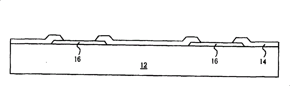
[0036] Step S100: providing a substrate, and sputtering a metal layer under the bump on the surface of the substrate;

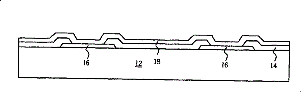
[0037] Step S200: etching the metal layer under the bump with a metal layer etchant;

[0038] Step S300: cleaning and drying the metal layer under the bump;

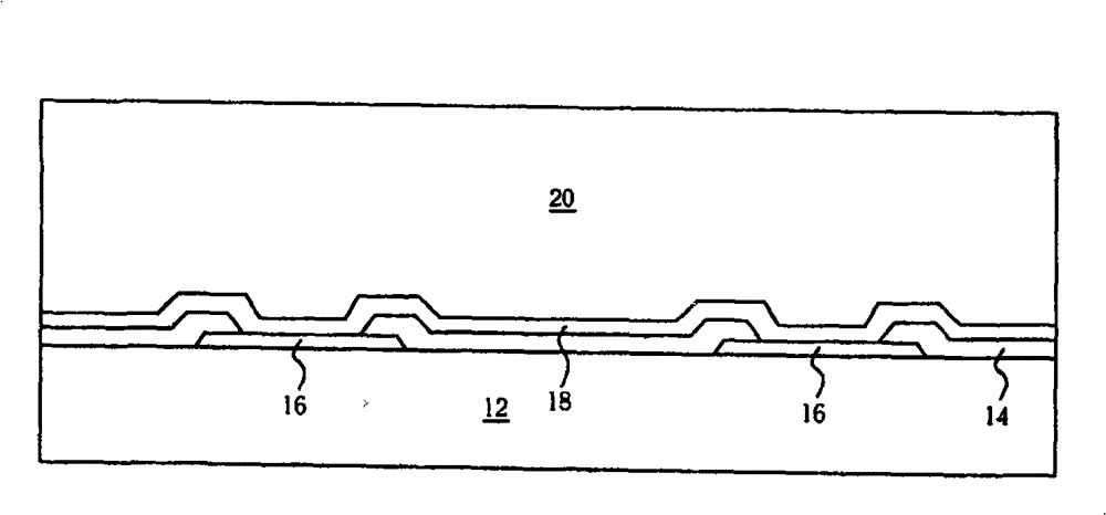
[0039] Step S400: forming a dry film pho...


PUM

PropertyMeasurementUnit
thicknessaaaaaaaaaa

Abstract

The invention provides a method for forming welding convex blocks, which comprises the following steps: providing a substrate, wherein a convex block lower metal layer is formed on the surface of the substrate; using the metal layer etching liquid for etching the convex block lower metal layer; cleaning and drying the convex block lower metal layer; and forming welding convex blocks on the convex block lower metal layer. The invention carries out short-time etching through the metal etching liquid, and can carry out micro etching on the surface of the convex block lower metal layer, so the microscopic structure on the surface can be changed, and the roughness is improved, the adhesive force between the convex blocks and dry film photo resistors can be enhanced, and the phenomenon of diffusion coating can not occur. Thereby, the performance and the quality of a chip can be improved.

Description

technical field [0001] The present invention relates to a method of wafer bonding, and in particular, to a method of forming bonding bumps. Background technique [0002] With the rapid development of science and technology and the high development of the semiconductor industry, electronic products composed of semiconductor components have become an indispensable tool in the daily life of modern people. In order to follow the trend of electronic products toward light, thin and short designs, the semiconductor packaging technology has also developed many high-density semiconductor packaging forms, such as flip-chip packages. Flip chip in Package process has good electrical characteristics, high output / input contact density, and can reduce IC size to increase the output of each wafer (Wafer), and has been optimistic about the future packaging method with great potential. In flip chip technology, bumping becomes the key to the success or failure of flip chip technology. [000...

Claims


Application Information

Patent Timeline
Patent Type & Authority Patents(China)
IPC IPC(8): H05K3/34B23K35/24
Inventor 王重阳梅娜
Owner SEMICON MFG INT (SHANGHAI) CORP
Why Eureka
Try Eureka